AWT6277R
AWT6277R is Linear Power Amplifier Module manufactured by ANADIGICS.
FEATURES
- - In Ga P HBT Technology High Efficiency: 44% @ POUT = +28.5 d Bm 21% @ POUT = +16 d Bm 16% @ POUT = +7 d Bm
- -
- -
- -
- -
- Low Quiescent Current: 15 m A Low Leakage Current in Shutdown Mode: <1 µA VREF = +2.85 V (+2.75 V min over temp) Optimized for a 50 Ω System Low Profile Miniature Surface Mount Package Option: 1.1 mm Max Ro HS pliant Package Option, 250 o C MSL-3 HSDPA pliant (no backoff) Dual Band WCDMA Wireless Handsets Dual Mode 3GPP Wireless Handsets bias modes that optimize efficiency for different output power levels, and a shutdown mode with low leakage current, increase handset talk and standby time. The self-contained 4 mm x 4 mm x 1.1 mm surface mount package incorporates matching networks optimized for output power, efficiency, and linearity in a 50 Ω system.
M20 Package 10 Pin 4 mm x 4 mm x 1.1 mm Surface Mount Module
APPLICATIONS
PRODUCT DESCRIPTION
The AWT6277 meets the increasing demands for higher output power in UMTS handsets. The PA module is optimized for VREF = +2.85 V, a requirement for patibility with the Qualm® 6250 chipset. The device is manufactured on an advanced In Ga P HBT MMIC technology offering state-of-the-art reliability, temperature stability, and ruggedness. Selectable
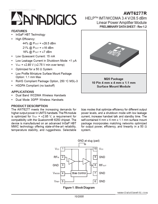
GND at slug (pad) VCC RFIN GND
1 2 3 Bias Control 10 VCC 9 8 7 6
GND RFOUT GND GND
VMODE 4 VREF 5
Figure 1: Block Diagram
10/2005
..
GND VCC RFIN GND VMODE VREF 1 2 3 4 5 GND
10 VCC 9 8 7 6 GND RFOUT GND GND
Figure 2: Pinout (X-ray Top View)
Table 1: Pin Description
PIN 1 2 3 4 5 6 7 8 9 10 NAME V CC RFIN GND VMODE VREF GND GND RFOUT GND V CC DESCRIPTION
Supply Voltage RF Input Ground Mode Control Voltage Reference Voltage Ground Ground RF Output Ground Supply Voltage
PRELIMINARY DATA SHEET
- Rev 1.2 10/2005
..
ELECTRICAL CHARACTERISTICS
Table 2: Absolute Minimum and Maximum Ratings
PARAMETER Supply Voltage (VCC) Mode Control Voltage (VMODE) Reference Voltage (VREF) RF Input Power (PIN) Storage Temperature...