AWT6332
AWT6332 is LINEAR POWER AMPLIFIER manufactured by ANADIGICS.
FEATURES
APPLICATIONS
- CDMA/EVDO PCS-band Wireless Handsets and Data Devices
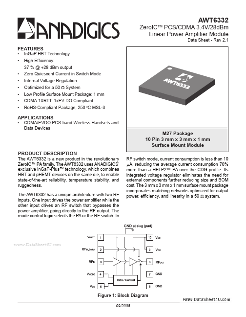
M27 Package 10 Pin 3 mm x 3 mm x 1 mm Surface Mount Module
RF switch mode, current consumption is less than 10 A, reducing the average current consumption 70% more than a HELP2™ PA over the CDG profile. Its integrated voltage regulator eliminates the need for external ponents further reducing size and BOM cost. The 3 mm x 3 mm x 1 mm surface mount package incorporates matching networks optimized for output power, efficiency, and linearity in a 50 system.
PRODUCT DESCRIPTION
The AWT6332 is a new product in the revolutionary Zero IC™ PA family. The AWT6332 uses ANADIGICS’ exclusive In Ga P-Plus™ technology, which bines HBT and p HEMT devices on the same die, to enable state-of-the-art reliability, temperature stability, and ruggedness. The AWT6332 has a unique architecture with two RF inputs. One input drives the power amplifier while the other input drives an RF switch that bypasses the power amplifier, going directly to the RF output. The mode control logic selects the PA or the RF switch. In
..
Figure 1: Block Diagram
09/2008
Figure 2: Pinout (X-ray Top View)
Table 1: Pin Description
PIN 1 2 3 4 5 6 7 8 9 10 NAME VBATT RFIN_SWITCH RFIN_PA VMODE VEN GND GND RFOUT VCC VCC DESCRIPTION
Battery Voltage RF Input to Switch RF Input to PA Mode Control Voltage PA Enable Voltage Ground Ground RF Output Supply Voltage Supply Voltage
..
Data Sheet
- Rev 2.1 09/2008
ELECTRICAL CHARACTERISTICS
Table 2: Absolute Minimum and Maximum Ratings
PARAMETER Supply Voltage (VCC and VBATT) Mode Control Voltage (VMODE) Enable Voltage (VEN) RF Input Power (PIN) to PA RF Input Power (PIN) to Switch Storage Temperature (TSTG) MIN 0 0 0 -40 MAX +5 +3.5 +3.5 +10 +20 +150 UNIT V V V d Bm d Bm °C
Stresses in excess of the absolute ratings may cause permanent damage. Functional operation is not implied under these conditions. Exposure to absolute ratings for extended periods of time may...