AWT6302R
AWT6302R is LINEAR POWER AMPLIFIER manufactured by ANADIGICS.
PCS/CDMA 3.4V/28dBm Linear Power Amplifier Module
Features
- InGaP HBT Technology
- High Efficiency: 39%, VMODE = 0 V 40%, VMODE = +2.85 V (no mode switching)
- Low Quiescent Current: 50 mA
- Low Leakage Current in Shutdown Mode: <1 µA
- VREF = +2.85 V (+2.75 V min over temp)
- Optimized for a 50 Ω System
- Low Profile Miniature Surface Mount Package: 1.1 mm
- CDMA 1XRTT, 1xEV-DO pliant
- Pinout Enables Easy Phone Board Migration From 4 mm x 4 mm Package
- RoHS-pliant Package, 250 oC MSL-3
Data Sheet
- Rev 2.1
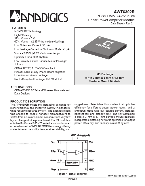
M9 Package 8 Pin 3 mm x 3 mm x 1.1 mm Surface Mount Module
APPLICATIONS
- CDMA/EVDO PCS-band Wireless Handsets and Data Devices
PRODUCT...