Datasheet Details
| Part number | AP2302AGN-HF |
|---|---|
| Manufacturer | Advanced Power Electronics Corp |
| File Size | 90.45 KB |
| Description | N-channel Enhancement-mode Power MOSFET |
| Datasheet | AP2302AGN-HF-AdvancedPowerElectronics.pdf |
|
|
|
Overview: AP2302AGN-HF Halogen-Free Product Advanced Power Electronics Corp. ▼ Capable of 2.5V gate drive ▼ Lower Gate Charge ▼ Surface mount package ▼ RoHS Compliant & Halogen-Free SOT-23 D N-CHANNEL ENHANCEMENT MODE POWER MOSFET BVDSS RDS(ON) ID S G 20V 42mΩ 4.
| Part number | AP2302AGN-HF |
|---|---|
| Manufacturer | Advanced Power Electronics Corp |
| File Size | 90.45 KB |
| Description | N-channel Enhancement-mode Power MOSFET |
| Datasheet | AP2302AGN-HF-AdvancedPowerElectronics.pdf |
|
|
|
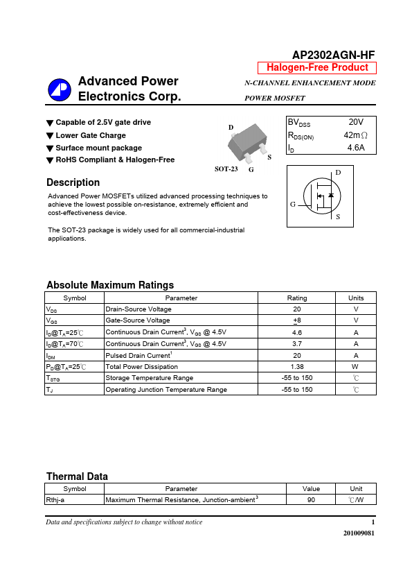
Advanced Power MOSFETs utilized advanced processing techniques to achieve the lowest possible on-resistance, extremely efficient and cost-effectiveness device.
The SOT-23 package is widely used for all commercial-industrial applications.
G S Absolute Maximum Ratings Symbol VDS VGS ID@TA=25℃ ID@TA=70℃ IDM PD@TA=25℃ TSTG TJ Parameter Drain-Source Voltage Gate-Source Voltage Continuous Drain Current , VGS @ 4.5V Continuous Drain Current , VGS @ 4.5V Pulsed Drain Current 1 3 3 Rating 20 +8 4.6 3.7 20 1.38 -55 to 150 -55 to 150 Units V V A A A W ℃ ℃ Total Power Dissipation Storage Temperature Range Operating Junction Temperature Range Thermal Data Symbol Rthj-a Parameter Maximum Thermal Resistance, Junction-ambient 3 Value 90 Unit ℃/W 1 201009081 Data and specifications subject to change without notice AP2302AGN-HF Electrical Characteristics@Tj=25oC(unless otherwise specified) Symbol BVDSS RDS(ON) VGS(th) gfs IDSS IGSS Qg Qgs Qgd td(on) tr td(off) tf Ciss Coss Crss Rg Parameter Drain-Source Breakdown Voltage Static Drain-Source On-Resistance2 Gate Threshold Voltage Forward Transconductance Drain-Source Leakage Current Gate-Source Leakage Total Gate Charge2 Gate-Source Charge Gate-Drain ("Miller") Charge Turn-on Delay Time Rise Time Turn-off Delay Time Fall Time Input Capacitance Output Capacitance Reverse Transfer Capacitance Gate Resistance 2 Test Conditions VGS=0V, ID=250uA VGS=4.5V, ID=4A VGS=2.5V, ID=3A VDS=VGS, ID=250uA VDS=5V, ID=4A VDS=16V, VGS=0V VGS=+8V, VDS=0V ID=4A VDS=10V VGS=4.5V VDS=10V ID=1A RG=3.3Ω VGS=5V VGS=0V VDS=20V f=1.0MHz f=1.0MHz Min.
| Brand Logo | Part Number | Description | Manufacturer |
|---|---|---|---|
| AP2302 | 3A DDR TERMINATION REGULATOR | BCD Semiconductor | |
| AP2302L | 2A DDR TERMINATION REGULATOR | BCD Semiconductor |
| Part Number | Description |
|---|---|
| AP2302AGN-HF-3 | N-channel Enhancement-mode Power MOSFET |
| AP2302GN | N-CHANNEL ENHANCEMENT MODE POWER MOSFET |
| AP2302GN-HF | N-channel Enhancement mode Power MOSFET |
| AP2302GN-HF-3 | N-channel Enhancement mode Power MOSFET |
| AP2302N | N-CHANNEL ENHANCEMENT MODE |
| AP2301AGN | P-CHANNEL ENHANCEMENT MODE POWER MOSFET |
| AP2301AGN-HF | P-CHANNEL ENHANCEMENT MODE POWER MOSFET |
| AP2301AGN-HF-3 | P-CHANNEL ENHANCEMENT MODE POWER MOSFET |
| AP2301BGN-HF | P-CHANNEL ENHANCEMENT MODE POWER MOSFET |
| AP2301EN-HF | P-CHANNEL ENHANCEMENT MODE POWER MOSFET |