Datasheet Details
| Part number | AP4511GED |
|---|---|
| Manufacturer | Advanced Power Electronics Corp |
| File Size | 116.15 KB |
| Description | N AND P-CHANNEL ENHANCEMENT MODE POWER MOSFET |
| Datasheet | AP4511GED-AdvancedPowerElectronics.pdf |
|
|
|
Overview: Advanced Power Electronics Corp. AP4511GED Pb Free Plating Product N AND P-CHANNEL ENHANCEMENT MODE POWER MOSFET ▼ Simple Drive Requirement ▼ Lower Gate Charge ▼ Fast Switching Performance ▼ RoHS pliant D2 D2 D1 D1.
| Part number | AP4511GED |
|---|---|
| Manufacturer | Advanced Power Electronics Corp |
| File Size | 116.15 KB |
| Description | N AND P-CHANNEL ENHANCEMENT MODE POWER MOSFET |
| Datasheet | AP4511GED-AdvancedPowerElectronics.pdf |
|
|
|
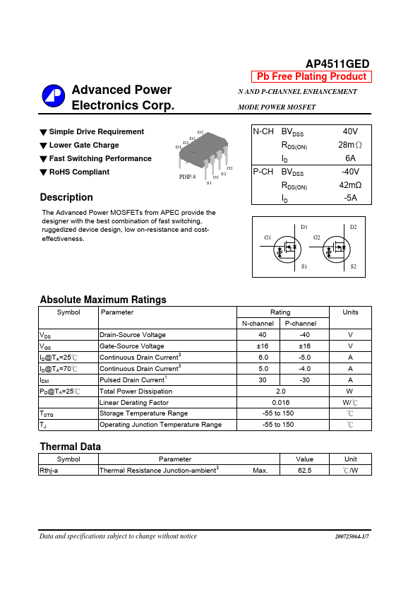
The Advanced Power MOSFETs from APEC provide the designer with the best bination of fast switching, ruggedized device design, low on-resistance and costeffectiveness.
N-CH P-CH BVDSS RDS(ON) ID BVDSS RDS(ON) ID 40V 28mΩ 6A -40V 42mΩ -5A D1 D2 G1 G2 S1 S2 Absolute Maximum Ratings Symbol Parameter VDS VGS ID@TA=25℃ ID@TA=70℃ IDM PD@TA=25℃ TSTG TJ Drain-Source Voltage Gate-Source Voltage Continuous Drain Current3 Continuous Drain Current3 Pulsed Drain Current1 Total Power Dissipation Linear Derating Factor Storage Temperature Range Operating Junction Temperature Range Thermal Data Symbol Parameter Rthj-a Thermal Resistance Junction-ambient3 Rating N-channel P-channel 40 -40 ±16 ±16 6.0 -5.0 5.0 -4.0 30 -30 2.0 0.016 -55 to 150 -55 to 150 Max.
Value 62.5 Units V V A A A W W/℃ ℃ ℃ Unit ℃/W Data and specifications subject to change without notice 200725064-1/7 AP4511GED N-CH Electrical Characteristics@ Tj=25oC(unless otherwise specified) Symbol BVDSS ΔBVDSS/ΔTj RDS(ON) VGS(th) gfs IDSS IGSS Qg Qgs Qgd td(on) tr td(off) tf Ciss Coss Crss Rg Parameter Test Conditions Drain-Source Breakdown Voltage VGS=0V, ID=250uA Breakdown Voltage Temperature Coefficient Reference to 25℃, ID=1mA Static Drain-Source On-Resistance2 VGS=10V, ID=6A VGS=4.5V, ID=4A Gate Threshold Voltage VDS=VGS, ID=250uA Forward Transconductance Drain-Source Leakage Current (Tj=25oC) Drain-Source Leakage Current (Tj=70oC) Gate-Source Leakage Total Gate Charge2 Gate-Source Charge Gate-Drain ("Miller") Charge Turn-on Delay Time2 Rise Time Turn-off Delay Time Fall Time Input Capacitance Output Capacitance Reverse Transfer Capacitance VDS=10V, ID=6A VDS=40V, VGS=0V VDS=32V, VGS=0V VGS=±16V ID=6A VDS=20V VGS=4.5V VDS=20V ID=6A
| Part Number | Description |
|---|---|
| AP4511GED-HF | N AND P-CHANNEL ENHANCEMENT MODE POWER MOSFET |
| AP4511GD | N AND P-CHANNEL ENHANCEMENT MODE POWER MOSFET |
| AP4511GH | N AND P-CHANNEL ENHANCEMENT MODE POWER MOSFET |
| AP4511GH-A | N AND P-CHANNEL ENHANCEMENT MODE POWER MOSFET |
| AP4511GH-HF | N AND P-CHANNEL ENHANCEMENT MODE POWER MOSFET |
| AP4511GM | N AND P-CHANNEL ENHANCEMENT MODE POWER MOSFET |
| AP4511GM-HF | N AND P-CHANNEL ENHANCEMENT MODE POWER MOSFET |
| AP4513GD | N AND P-CHANNEL ENHANCEMENT MODE POWER MOSFET |
| AP4513GH | N AND P-CHANNEL ENHANCEMENT MODE POWER MOSFET |
| AP4513GM | N AND P-CHANNEL ENHANCEMENT MODE POWER MOSFET |