AP9920GEO
Overview
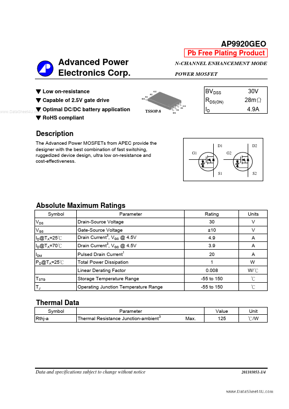
The Advanced Power MOSFETs from APEC provide the designer with the best combination of fast switching, ruggedized device design, ultra low on-resistance and cost-effectiveness.
| Part | AP9920GEO |
|---|---|
| Description | N-CHANNEL ENHANCEMENT MODE POWER MOSFET |
| Category | MOSFET |
| Manufacturer | Advanced Power Electronics Corp |
| Size | 140.82 KB |
The Advanced Power MOSFETs from APEC provide the designer with the best combination of fast switching, ruggedized device design, ultra low on-resistance and cost-effectiveness.
| Part Number | Manufacturer | Description |
|---|---|---|
| AP9563GH | Advanced Power Electronics Corp | P-CHANNEL ENHANCEMENT MODE POWER MOSFET |
| FCPF360N65S3R0L | onsemi | N-Channel MOSFET |
| A2SHB | HAOHAI | N-Channel MOSFET |