AFC2517W
AFC2517W is N & P-Channel Enhancement Mode MOSFET manufactured by Alfa-MOS.
- Part of the AFC2517W-Alfa comparator family.
- Part of the AFC2517W-Alfa comparator family.
Description
AFC2517W, N & P Pair enhancement mode MOSFET, uses Advanced Trench Technology to provide excellent RDS(ON), low gate charge. These devices are particularly suited for low voltage power management, and low in-line power loss are needed in mercial industrial surface mount applications.
20V N & P Pair Enhancement Mode MOSFET
Features z N-Channel 20V/4.6A,RDS(ON)=25mΩ@VGS=4.5V 20V/4.2A,RDS(ON)=30mΩ@VGS=2.5V 20V/3.8A,RDS(ON)=38mΩ@VGS=1.8V z P-Channel -20V/-3.6A,RDS(ON)=52mΩ@VGS=4.5V -20V/-3.2A,RDS(ON)=65mΩ@VGS=2.5V -20V/-1.2A,RDS(ON)=82mΩ@VGS=1.8V z Super high density cell design for extremely low RDS (ON) z Exceptional on-resistance and maximum DC current capability z DFN2X2-6L package design
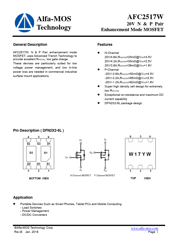
Pin Description
( DFN2X2-6L )
Application z Portable Devices Such as Smart Phones, Tablet PCs and Mobile puting
- Load Switches
- Power Management
- DC/DC Converters
©Alfa-MOS Technology Corp. Rev.B Jan. 2018
.alfa-mos.
Pag...