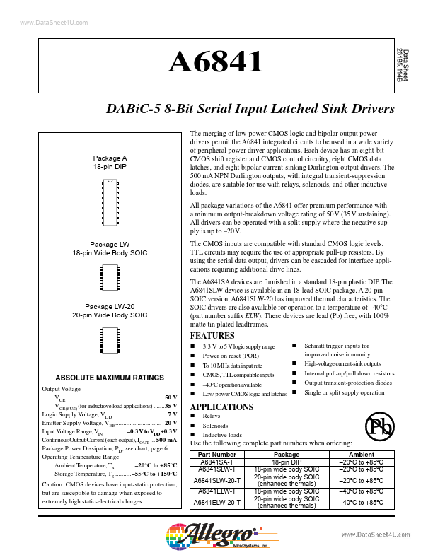
A6841
A6841 is DABiC-5 8-Bit Serial Input Latched Sink Drivers manufactured by Allegro MicroSystems.
..
Data Sheet 26185.114B
DABiC-5 8-Bit Serial Input Latched Sink Drivers
The merging of low-power CMOS logic and bipolar output power drivers permit the A6841 integrated circuits to be used in a wide variety of peripheral power driver applications. Each device has an eight-bit CMOS shift register and CMOS control circuitry, eight CMOS data latches, and eight bipolar current-sinking Darlington output drivers. The 500 mA NPN Darlington outputs, with integral transient-suppression diodes, are suitable for use with relays, solenoids, and other inductive loads. All package variations of the A6841 offer premium performance with a minimum output-breakdown voltage rating...