AS7C251MNTD36A
AS7C251MNTD36A is 2.5V 1M x 32/36 Pipelined SRAM manufactured by Alliance Semiconductor Corporation.
- Part of the AS7C251MNTD32A comparator family.
- Part of the AS7C251MNTD32A comparator family.
Features
- Organization: 1,048,576 words × 32 or 36 bits
- NTD™architecture for efficient bus operation
- Fast clock speeds to 200 MHz
- Fast clock to data access: 3.2/3.5/3.8 ns
- Fast OE access time: 3.2/3.5/3.8 ns
- Fully synchronous operation
- pipelined mode ..
- mon data inputs and data outputs
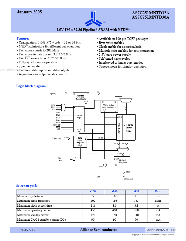
- Asynchronous output enable control Logic block diagram
A[19:0] 20 D
- Available in 100-pin TQFP packages
- Byte write enables
- Clock enable for operation hold
- Multiple chip enables for easy expansion
- 2.5V core power supply
- Self-timed write cycles
- Interleaved or linear burst modes
- Snooze mode for standby operation
Address register Burst logic
CLK CE0 CE1 CE2 R/W BWa BWb BWc BWd ADV / LD LBO ZZ
Q 20
Write delay addr. registers
Control logic
Write Buffer
1M x 32/36 SRAM Array
DQ[a,b,c,d]
32/36
Data Q Input Register
32/36 32/36 32/36
32/36 CLK CEN CLK OE
Output Register
32/36...