AS7C33256PFD36A
AS7C33256PFD36A is 3.3V 256K x 32/36 pipelined burst synchronous SRAM manufactured by Alliance Semiconductor Corporation.
- Part of the AS7C33256PFD32A comparator family.
- Part of the AS7C33256PFD32A comparator family.
December 2004
®
AS7C33256PFD32A AS7C33256PFD36A
3.3V 256K × 32/36 pipelined burst synchronous SRAM
Features
- -
- -
- -
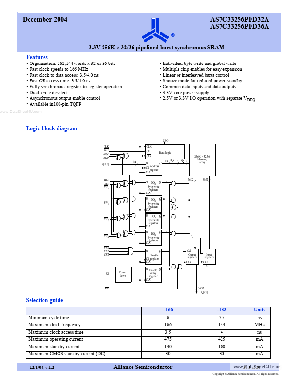
- - Organization: 262,144 words x 32 or 36 bits Fast clock speeds to 166 MHz Fast clock to data access: 3.5/4.0 ns Fast OE access time: 3.5/4.0 ns Fully synchronous register-to-register operation Dual-cycle deselect Asynchronous output enable control Available in100-pin TQFP
- -
- -
- -
- Individual byte write and global write Multiple chip enables for easy expansion Linear or interleaved burst control Snooze mode for reduced power-standby mon data inputs and data outputs 3.3V core power supply 2.5V or 3.3V I/O operation with separate VDDQ
..
Logic...