AS7C33256PFS18A
AS7C33256PFS18A is 3.3V 256K X 16/18 pipeline burst synchronous SRAM manufactured by Alliance Semiconductor Corporation.
- Part of the AS7C33256PFS16A comparator family.
- Part of the AS7C33256PFS16A comparator family.
March 2001
®
AS7C33256PFS16A AS7C33256PFS18A
3.3V 256K × 16/18 pipeline burst synchronous SRAM
Features
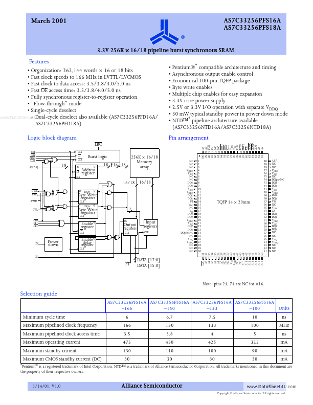
- Organization: 262,144 words × 16 or 18 bits
- Fast clock speeds to 166 MHz in LVTTL/LVCMOS
- Fast clock to data access: 3.5/3.8/4.0/5.0 ns
- Fast OE access time: 3.5/3.8/4.0/5.0 ns
- Fully synchronous register-to-register operation
- “Flow-through” mode
- Single-cycle deselect
- Dual-cycle deselect also available (AS7C33256PFD16A/ .. AS7C33256PFD18A)
- Pentium®- patible architecture and timing
- Asynchronous output enable control
- Economical 100-pin TQFP package
- Byte write enables
- Multiple chip enables for easy expansion
- 3.3V core power supply
- 2.5V or...