FEATURES
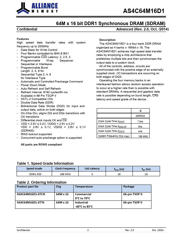
High speed data transfer rates with system frequency up to 200MHz - Data Mask for Write Control - Four Banks controlled by BA0 & BA1 - Programmable CAS Latency: 2, 2.5, 3 - Programmable Wrap Sequence: Sequential or Interleave - Programmable Burst Length: 2, 4, 8 for Sequential Type 2, 4, 8 for Interleave Type - Automatic and Controlled Precharge Command - Power Down Mode - Auto Refresh and Self Refresh - Refresh Interval: 8192 cycles/64 ms - Available in 66 Pin TSOP II - SSTL-2 Compatible I/Os - Double Data Rate (DDR) - Bidirectional Data Strobe (DQS) for input and output data, active on both edges - On-Chip DLL aligns DQ and DQs transitions with CK transitions - CK - VDD = 2.5V ± 0.2V, VDDQ = 2.5V ± 0.2V VDD = 2.6V ± 0.1V, VDDQ = 2.6V ± 0.1V (DDR400) - tRAS lockout supported - Concurrent auto precharge option is supported All parts are ROHS compliant DESCRIPTION
All of the controls, address, circuits are synchronized with the positive edge of an externally supplied clock. I/O transactions are occurring on both edges of DQS. Alliance Semiconductor