Datasheet4U Logo Datasheet4U.com

AS4C64M16D1A-6TIN - 1Gb SDRAM

General Description

Table 2.

Differential Clock: CK and CK are differential clock inputs.

All address and control input signals are sampled on the crossing of the positive edge of CK and negative edge of CK .

Key Features

  • Overview.
  • Fast clock rate: 166MHz.
  • Differential Clock CK & CK.
  • Bi-directional DQS.
  • DLL enable/disable by EMRS.
  • Fully synchronous operation.
  • Internal pipeline architecture.
  • Four internal banks, 16M x 16-bit for each bank.
  • Programmable Mode and Extended Mode registers - CAS Latency: 2, 2.5, 3 - Burst length: 2, 4, 8 - Burst Type: Sequential & Interleaved.
  • Individual byte write mask control.
  • DM Write Latency.

📥 Download Datasheet

Datasheet Details

Part number AS4C64M16D1A-6TIN
Manufacturer Alliance Semiconductor
File Size 1.48 MB
Description 1Gb SDRAM
Datasheet download datasheet AS4C64M16D1A-6TIN Datasheet

Full PDF Text Transcription (Reference)

The following content is an automatically extracted verbatim text from the original manufacturer datasheet and is provided for reference purposes only.

View original datasheet text
  AS4C64M16D1A   
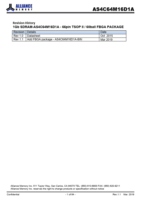
Revision History 1Gb SDRAM-AS4C64M16D1A - 66pin TSOP II / 60ball FBGA PACKAGE Revision Details Rev 1.0 Datasheet Rev 1.1 Add FBGA package - AS4C64M16D1A-BIN Date Oct 2015 Mar 2019 Alliance Memory Inc. 511 Taylor Way, San Carlos, CA 94070 TEL: (650) 610-6800 FAX: (650) 620-9211 Alliance Memory Inc. reserves the right to change products or specification without notice Confidential - 1 of 64 - Rev.1.1 Mar. 2019 AS4C64M16D1A Features Overview • Fast clock rate: 166MHz • Differential Clock CK & CK • Bi-directional DQS • DLL enable/disable by EMRS • Fully synchronous operation • Internal pipeline architecture • Four internal banks, 16M x 16-bit for each bank • Programmable Mode and Extended Mode registers - CAS Latency: 2, 2.