AS4LC1M16E5
AS4LC1M16E5 is 3V 1M x 16 CMOS DRAM manufactured by Alliance Semiconductor.
®
3V 1M×16 CMOS DRAM (EDO)
Features
- Organization: 1,048,576 words × 16 bits
- High speed
- 50/60 ns RAS access time
- 20/25 ns hyper page cycle time
- 12/15 ns CAS access time
- Low power consumption
- Active: 500 mW max (-60)
- Standby: 3.6 mW max, CMOS DQ
- Extended data out
- 1024 refresh cycles, 16 ms refresh interval
- RAS-only or CAS-before-RAS refresh or self-refresh
- Read-modify-write
- TTL-patible, three-state DQ
- JEDEC standard package and pinout
- 400 mil, 42-pin SOJ
- 400 mil, 44/50-pin TSOP II
- 3V power supply (AS4LC1M16E5)
- 5V tolerant I/Os; 5.5V maximum VIH
- Industrial and mercial temperature available
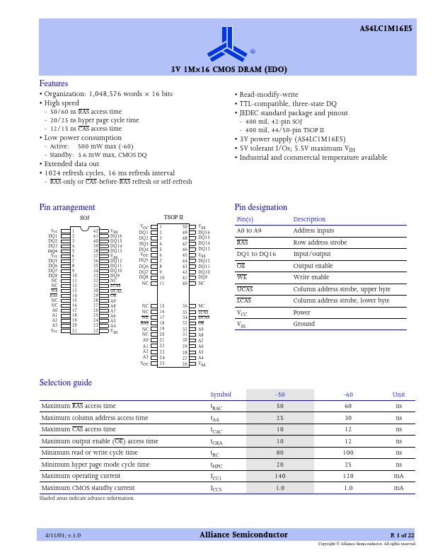
Pin arrangement
Vcc DQ1 DQ2 DQ3 DQ4...