Datasheet4U Logo Datasheet4U.com

AS4LC2M8S0 - (AS4LCxMxxSx) 3.3V 2M X 8/1M X 16 CMOS synchronous DRAM

Description

Output disable/write mask AS4LC2M8S1 and AS4LC2M8S0 AS4LC1M16S0 and AS4LC1M16S1 DataSheet4U.com VSSQ DQ9 DQ8 VCCQ NC UDQM CLK CKE NC A9 A8 A7 A6 A5 A4 VSS RA0 10 DataShee Address inputs CA0 7 (×16) CA0 8 (×8) Bank address (BA) Input/output Row address strobe Column

Features

  • Organization - 1,048,576 words × 8 bits × 2 banks (2M × 8) 11 row, 9 column address - 524,288 words × 16 bits × 2 banks (1M × 16) 11 row, 8 column address AS4LC2M8S1 AS4LC2M8S0 AS4LC1M16S1 AS4LC1M16S0.
  • All signals referenced to positive edge of clock, fully synchronous.
  • Dual internal banks controlled by A11 (bank select).
  • High speed - 143/125/100 MHz - 7/8/10 ns clock access time.
  • Auto refresh and self refresh.
  • PC100 functionality.

📥 Download Datasheet

Datasheet preview – AS4LC2M8S0

Datasheet Details

Part number AS4LC2M8S0
Manufacturer Alliance Semiconductor
File Size 1.01 MB
Description (AS4LCxMxxSx) 3.3V 2M X 8/1M X 16 CMOS synchronous DRAM
Datasheet download datasheet AS4LC2M8S0 Datasheet
Additional preview pages of the AS4LC2M8S0 datasheet.
Other Datasheets by Alliance Semiconductor

Full PDF Text Transcription

Click to expand full text
www.DataSheet4U.com May 2001 Preliminary ® 
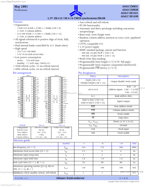
3.3V 2M × 8/1M × 16 CMOS synchronous DRAM Features • Organization - 1,048,576 words × 8 bits × 2 banks (2M × 8) 11 row, 9 column address - 524,288 words × 16 bits × 2 banks (1M × 16) 11 row, 8 column address AS4LC2M8S1 AS4LC2M8S0 AS4LC1M16S1 AS4LC1M16S0 • All signals referenced to positive edge of clock, fully synchronous • Dual internal banks controlled by A11 (bank select) • High speed - 143/125/100 MHz - 7/8/10 ns clock access time • Auto refresh and self refresh • PC100 functionality • Automatic and direct precharge including concurrent autoprecharge • Burst read, write/Single write • Random column address assertion in every cycle, pipelined operation • LVTTL compatible I/O • 3.
Published: |