Alliance Semiconductor AS7C33256NTD16A
The AS7C33256NTD16A/18A family is a high performance CMOS 4-Mbit synchronous Static Random Access Memory (SRAM) organized as 262,144 words × 16 or 18 bits and incorporates a LATE LATE Write. This variation of the 4Mb sychronous SRAM uses the No Turnaround Delay (NTD) architecture, featuring an enhanced Write operation that improves bandwidth over pipelined burst devices. These dead cycles can significantly reduce overall bandwidth for applications requiring random access or Read-ModifyWrite operations.| Part No. | AS7C33256NTD16A |
|---|---|
| Datasheet | AS7C33256NTD16A Download |
| Manufacturer |  Alliance Semiconductor |
| Description | 3.3V 256K X 16/18 SRAM |
| Buy | Stock & Price |
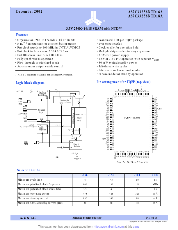
FEATURES
● Organization: 262,144 words × 16 or 18 bits● NTD™1 architecture for efficient bus operation
● Fast clock speeds to 166 MHz in LVTTL/LVCMOS
● Fast clock to data access: 3.5/4.0/5.0 ns
● Fast OE access time: 3.5/4.0/5.0 ns
● Fully synchronous operation
● Flow-through or pipelined mode
● Asynchronous output enable control 1 NTD is a trademark of Alliance Semiconductor Corporation.
● Economical 100-pin TQFP package
● Byte write enables
● Clock enable for operation hold
● Multiple chip enables for easy expansion
● 3.3V core power supply
● 2.5V or 3.3V I/O operation with separate VDDQ
● 30 mW typical standby power
● Self-timed write cycles
● Interleaved or linear burst modes
● Snooze mode for standby operation Logic block diagram Pin arrangement for TQFP (top view) A A CE0 CE1 NC NC BWb BWa CE2 VDD VSS CLK R/W CEN OE ADV/LD NC NC A A A[17:0] 18 CE0 CE1 CE2 R/W BWa BWb ADV / LD FT LBO ZZ D Aredgdirsetesrs Q Burst logic CLK Control logic CLK DQ [a:b] 16/18 D Data Q Input Register C...

