ASM5I2304B Overview
Key Features
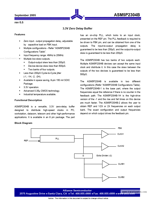
- output propagation delay, adjustable by capacitive load on FBK input. Multiple configurations
| Part | ASM5I2304B |
|---|---|
| Description | 3.3 V Zero Delay Buffer |
| Manufacturer | Alliance Semiconductor |
| Size | 396.17 KB |
| Part Number | Manufacturer | Description |
|---|---|---|
| BUF04 | Analog Devices | Closed-Loop High Speed Buffer |
| 74HC125 | NXP Semiconductors | Quad buffer/line driver |
| BUF03 | Analog Devices | High Speed Voltage Follower/Buffer |