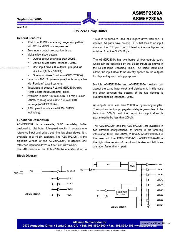
Datasheet4U Logo Datasheet4U.com

ASM5I2309A - (ASM5I2305A / ASM5I2309A) 3.3 V Zero Delay Buffer

Download the ASM5I2309A datasheet PDF. This datasheet also covers the ASM5I2305A variant, as both devices belong to the same (asm5i2305a / asm5i2309a) 3.3 v zero delay buffer family and are provided as variant models within a single manufacturer datasheet.

General Description

ASM5P2309A is a versatile, 3.3V zero-delay buffer designed to distribute high-speed clocks.

It accepts one reference input and drives out nine low-skew clocks.

It is available in a 16-pin package.

Key Features

  • 15MHz to 133MHz operating range, compatible with CPU and PCI bus frequencies. Zero input - output propagation delay. Multiple low-skew outputs.
  • www. DataSheet4U. com.
  • ASM5P2309A ASM5P2305A 133MHz frequencies, and has higher drive than the -1 devices. All parts have on-chip PLLs that lock to an input clock on the REF pin. The PLL feedback is on-chip and is obtained from the CLKOUT pad. The ASM5P2309A has two banks of four outputs each, which can be controlled by.

📥 Download Datasheet

Note: The manufacturer provides a single datasheet file (ASM5I2305A_AllianceSemiconductor.pdf) that lists specifications for multiple related part numbers.

Datasheet Details

Part number ASM5I2309A
Manufacturer Alliance Semiconductor
File Size 427.28 KB
Description (ASM5I2305A / ASM5I2309A) 3.3 V Zero Delay Buffer
Datasheet download datasheet ASM5I2309A Datasheet

Full PDF Text Transcription (Reference)

The following content is an automatically extracted verbatim text from the original manufacturer datasheet and is provided for reference purposes only.

View original datasheet text
September 2005 rev 1.6 3.3V Zero Delay Buffer General Features ƒ ƒ ƒ 15MHz to 133MHz operating range, compatible with CPU and PCI bus frequencies. Zero input - output propagation delay. Multiple low-skew outputs. ƒ ƒ www.DataSheet4U.com ƒ ASM5P2309A ASM5P2305A 133MHz frequencies, and has higher drive than the -1 devices. All parts have on-chip PLLs that lock to an input clock on the REF pin. The PLL feedback is on-chip and is obtained from the CLKOUT pad. The ASM5P2309A has two banks of four outputs each, which can be controlled by the Select inputs as shown in the Select Input Decoding Table. The select input also allows the input clock to be directly applied to the outputs for chip and system testing purposes.