Datasheet Details
| Part number | AOD4189 |
|---|---|
| Manufacturer | Alpha & Omega Semiconductors |
| File Size | 239.06 KB |
| Description | P-Channel MOSFET |
| Datasheet | AOD4189_AlphaOmegaSemiconductors.pdf |
|
|
Overview: AOD4189 P-Channel Enhancement Mode Field Effect Transistor General.
| Part number | AOD4189 |
|---|---|
| Manufacturer | Alpha & Omega Semiconductors |
| File Size | 239.06 KB |
| Description | P-Channel MOSFET |
| Datasheet | AOD4189_AlphaOmegaSemiconductors.pdf |
|
|
|
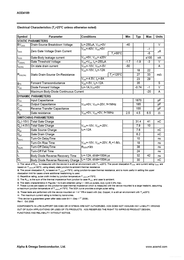
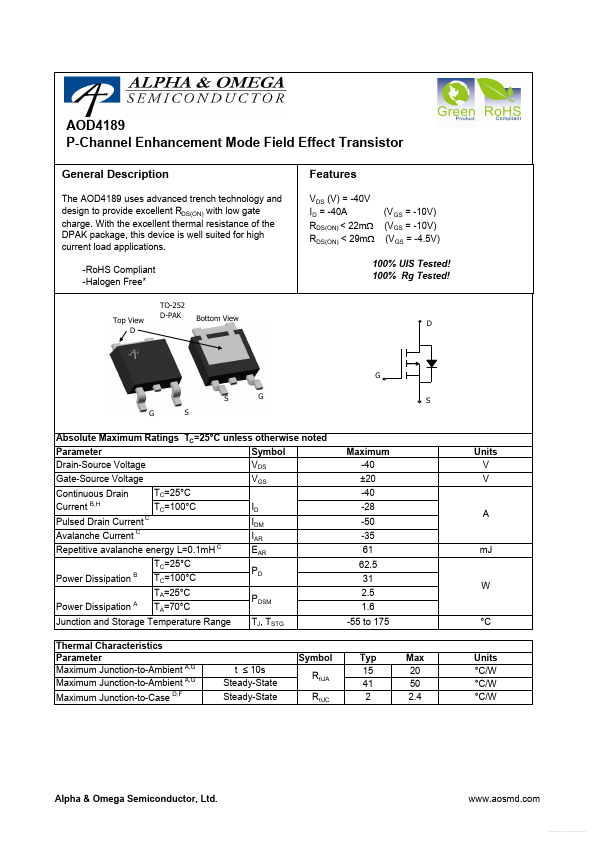
The AOD4189 uses advanced trench technology and design to provide excellent RDS(ON) with low gate charge.
With the excellent thermal resistance of the DPAK package, this device is well suited for high current load applications.
-RoHS Compliant -Halogen Free* TO-252 D-PAK
| Brand Logo | Part Number | Description | Manufacturer |
|---|---|---|---|
| AOD4189 | P-Channel MOSFET | INCHANGE | |
| AOD4189 | P-Channel MOSFET | VBsemi |
| Part Number | Description |
|---|---|
| AOD418 | 30V N-Channel MOSFET |
| AOD4180 | 80V N-Channel MOSFET |
| AOD4182 | 80V N-Channel MOSFET |
| AOD4184 | 40V N-Channel MOSFET |
| AOD4184A | 40V N-Channel MOSFET |
| AOD4185 | 40V P-Channel MOSFET |
| AOD4186 | 40V N-Channel MOSFET |
| AOD4187 | P-Channel MOSFET |
| AOD410 | N-Channel MOSFET |
| AOD4100 | N-Channel MOSFET |