Datasheet Details
| Part number | AOI452 |
|---|---|
| Manufacturer | Alpha & Omega Semiconductors |
| File Size | 470.64 KB |
| Description | N-Channel MOSFET |
| Datasheet |
 AOI452 Datasheet AOI452 Datasheet
|
|
|
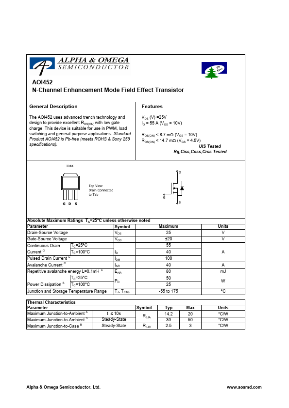
The AOI452 uses advanced trench technology and design to provide excellent RDS(ON) with low gate charge.
This device is suitable for use in PWM, load switching and general purpose applications.
Standard Product AOI452 is Pb-free (meets ROHS & Sony 259 specifications).
| Part number | AOI452 |
|---|---|
| Manufacturer | Alpha & Omega Semiconductors |
| File Size | 470.64 KB |
| Description | N-Channel MOSFET |
| Datasheet |
AOI452 Datasheet
|
|
|
|