Datasheet Details
| Part number | AON2801 |
|---|---|
| Manufacturer | Alpha & Omega Semiconductors |
| File Size | 297.64 KB |
| Description | Dual P-Channel MOSFET |
| Download | AON2801 Download (PDF) |
|
|
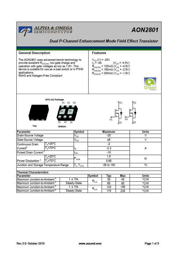
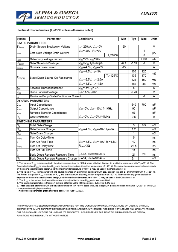
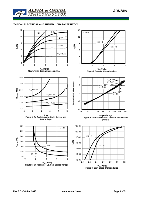
Overview: AON2801 Dual P-Channel Enhancement Mode Field Effect Transistor.
| Part number | AON2801 |
|---|---|
| Manufacturer | Alpha & Omega Semiconductors |
| File Size | 297.64 KB |
| Description | Dual P-Channel MOSFET |
| Download | AON2801 Download (PDF) |
|
|
|
The AON2801 uses advanced trench technology to provide excellent RDS(ON), low gate charge and operation with gate voltages as low as 1.8V.
This device is suitable for use as a load switch or in PWM applications.
RoHS and Halogen-Free Compliant
Compare AON2801 distributor prices and check real-time stock availability from major suppliers. Prices and inventory may vary by region and order quantity.
| Part Number | Description |
|---|---|
| AON2800 | 20V Dual N-Channel MOSFET |
| AON2802 | 30V Dual N-Channel MOSFET |
| AON2803 | 20V Dual P-Channel MOSFET |
| AON2809 | 12V Dual P-Channel MOSFET |
| AON2810 | 30V Dual N-Channel MOSFET |
| AON2812 | 30V Dual N-Channel MOSFET |
| AON2880 | 20V Dual N-Channel MOSFET |
| AON2240 | 40V N-Channel MOSFET |
| AON2260 | 60V N-Channel MOSFET |
| AON2290 | 100V N-Channel MOSFET |