Datasheet Details
| Part number | AON6596 |
|---|---|
| Manufacturer | Alpha & Omega Semiconductors |
| File Size | 336.62 KB |
| Description | 30V N-Channel MOSFET |
| Download | AON6596 Download (PDF) |
|
|
Overview: AON6596 30V N-Channel AlphaMOS General.
| Part number | AON6596 |
|---|---|
| Manufacturer | Alpha & Omega Semiconductors |
| File Size | 336.62 KB |
| Description | 30V N-Channel MOSFET |
| Download | AON6596 Download (PDF) |
|
|
|
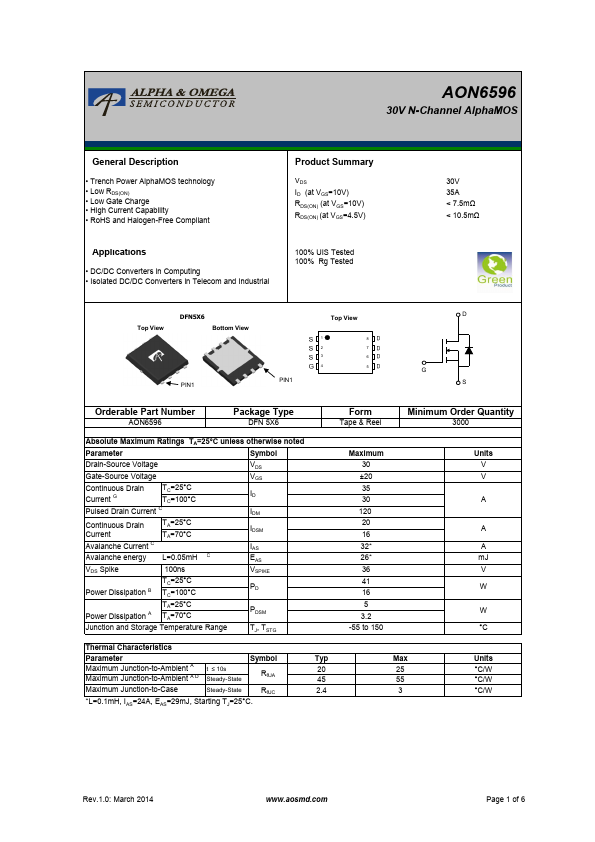
• Trench Power AlphaMOS technology • Low RDS(ON) • Low Gate Charge • High Current Capability • RoHS and Halogen-Free Compliant Product Summary VDS ID (at VGS=10V) RDS(ON) (at VGS=10V) RDS(ON) (at VGS=4.5V) Applications • DC/DC Converters in Computing • Isolated DC/DC Converters in Telecom and Industrial 100% UIS Tested 100% Rg Tested 30V 35A < 7.5mΩ < 10.5mΩ Top View DFN5X6 Bottom View PIN1 PIN1 Top View 1 8 2 7 3 6 4 5 D G S Orderable Part Number AON6596 Package Type DFN 5X6 Form Tape & Reel Minimum Order Quantity 3000 Absolute Maximum Ratings TA=25°C unless otherwise noted Parameter Symbol Drain-Source Voltage VDS Gate-Source Voltage VGS Continuous Drain Current G TC=25°C TC=100°C ID Pulsed Drain Current C IDM Continuous Drain Current TA=25°C TA=70°C IDSM Avalanche Current C IAS Avalanche energy LL==60m.0H5mH C EAS VDS Spike Power Dissipation B 100ns TC=25°C TC=100°C VSPIKE PD TA=25°C Power Dissipation A TA=70°C PDSM Junction and Storage Temperature Range TJ, TSTG Maximum 30 ±20 35 30 120 20 16 32* 26* 36 41 16 5 3.2 -55 to 150 Units V V A A A mJ V W W °C Thermal Characteristics Parameter Symbol Typ Maximum Junction-to-Ambient A t ≤ 10s Maximum Junction-to-Ambient A D Steady-State RθJA 20 45 Maximum Junction-to-Case Steady-State RθJC 2.4 *L=0.1mH, IAS=24A, EAS=29mJ, Starting TJ=25°C.
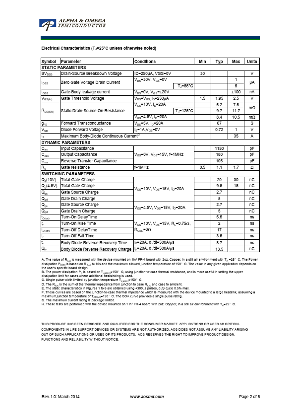
Max 25 55 3 Units °C/W °C/W °C/W Rev.1.0: March 2014 www.aosmd.com Page 1 of 6 Electrical Characteristics (TJ=25°C unless otherwise noted) Symbol Parameter Conditions Min STATIC PARAMETERS BVDSS Drain-Source Breakdown Voltage ID=250µA, VGS=0V 30 IDSS Zero Gate Voltage Drain Current VDS=30V, VGS=0V TJ=55°C IGSS Gate-Body leakage current VDS=0V, VGS=±20V VGS(th) Gate Threshold Voltage VDS=VGS, ID=250µA 1.5 VGS=10V, ID=20A RDS(ON) Static Drain-Source On-Resistance TJ=125°C VGS=4.5V, ID=20A gFS Forward Transconductance VDS=5V, ID=20A VSD Diode F
| Part Number | Description |
|---|---|
| AON6590 | 40V N-Channel MOSFET |
| AON6590A | 40V N-Channel MOSFET |
| AON6594 | 30V N-Channel MOSFET |
| AON6500 | N-Channel MOSFET |
| AON6502 | 30V N-Channel MOSFET |
| AON6504 | 30V N-Channel MOSFET |
| AON6506 | N-Channel MOSFET |
| AON6508 | N-Channel MOSFET |
| AON6510 | 30V N-Channel MOSFET |
| AON6512 | 30V N-Channel MOSFET |