Datasheet Details
| Part number | AON6810 |
|---|---|
| Manufacturer | Alpha & Omega Semiconductors |
| File Size | 347.46 KB |
| Description | N-Channel MOSFET |
| Download | AON6810 Download (PDF) |
|
|
Overview: AON6810 AlphaMOS 30V Common Drain N-Channel General.
| Part number | AON6810 |
|---|---|
| Manufacturer | Alpha & Omega Semiconductors |
| File Size | 347.46 KB |
| Description | N-Channel MOSFET |
| Download | AON6810 Download (PDF) |
|
|
|
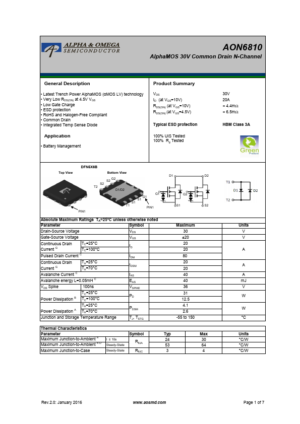
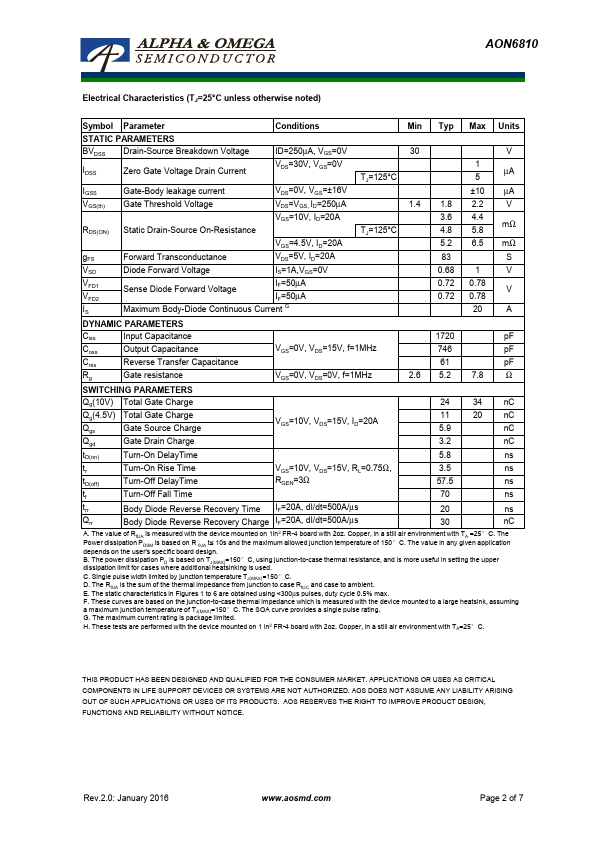
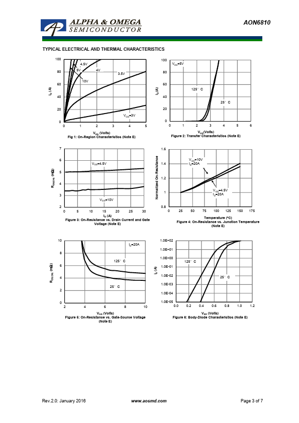
• Latest Trench Power AlphaMOS (αMOS LV) technology • Very Low RDS(ON) at 4.5V VGS • Low Gate Charge • ESD protection • RoHS and Halogen-Free Compliant • Common Drain • Integrated Temp Sense Diode Application • Battery Management Product Summary VDS ID (at VGS=10V) RDS(ON) (at VGS=10V) RDS(ON) (at VGS=4.5V) Typical ESD protection 100% UIS Tested 100% Rg Tested 30V 20A < 4.4mΩ < 6.5mΩ HBM Class 3A DFN5X6B Top View Bottom View G2 S2 S2 T2 D1/D2 D1 D2 G1 G2 G1 S1 S1 T1 PIN1 S1 S2 PIN1 Absolute Maximum Ratings TA=25°C unless otherwise noted Parameter Symbol Drain-Source Voltage VDS Gate-Source Voltage VGS Continuous Drain Current G TC=25°C TC=100°C ID Pulsed Drain Current C IDM Continuous Drain Current G TA=25°C TA=70°C IDSM Avalanche Current C IAS Avalanche energy L=0.05mH C EAS VDS Spike 100ns VSPIKE TC=25°C Power Dissipation B TC=100°C PD TA=25°C Power Dissipation A TA=70°C PDSM Junction and Storage Temperature Range TJ, TSTG Maximum 30 ±20 20 20 80 20 20 40 40 36 31 12.5 4.1 2.6 -55 to 150 Thermal Characteristics Parameter Symbol Typ Maximum Junction-to-Ambient A t ≤ 10s Maximum Junction-to-Ambient A D Steady-State RθJA 24 53 Maximum Junction-to-Case Steady-State RθJC 3 Max 30 64 4 Units V V A A A mJ V W W °C Units °C/W °C/W °C/W Rev.2.0: January 2016 www.aosmd.com Page 1 of 7 AON6810 Electrical Characteristics (TJ=25°C unless otherwise noted) Symbol Parameter Conditions Min Typ Max Units STATIC PARAMETERS BVDSS Drain-Source Breakdown Voltage ID=250µA, VGS=0V 30 V IDSS Zero Gate Voltage Drain Current VDS=30V, VGS=0V TJ=125°C 1 µA 5 IGSS Gate-Body leakage current VDS=0V, VGS=±16V ±10 µA VGS(th) Gate Threshold Voltage VDS=VGS, ID=250µA 1.4 1.8 2.2 V RDS(ON) Static Drain-Source On-Resistance VGS=10V, ID=20A TJ=125°C 3.6 4.4 mΩ 4.8 5.8 VGS=4.5V, ID=20A 5.2 6.5 mΩ gFS Forward Transconductance VDS=5V, ID=20A 83 S
| Part Number | Description |
|---|---|
| AON6812 | 30V Common Drain N-Channel MOSFET |
| AON6816 | 30V Dual N-Channel MOSFET |
| AON6850 | N-Channel MOSFET |
| AON6884 | N-Channel MOSFET |
| AON6144 | 40V N-Channel MOSFET |
| AON6152A | 45V N-Channel MOSFET |
| AON6154 | 45V N-Channel MOSFET |
| AON6156 | 45V N-Channel MOSFET |
| AON6160 | N-Channel MOSFET |
| AON6162 | 60V N-Channel MOSFET |