Datasheet Details
| Part number | AON7418 |
|---|---|
| Manufacturer | Alpha & Omega Semiconductors |
| File Size | 383.62 KB |
| Description | 30V N-Channel MOSFET |
| Download | AON7418 Download (PDF) |
|
|
| Part number | AON7418 |
|---|---|
| Manufacturer | Alpha & Omega Semiconductors |
| File Size | 383.62 KB |
| Description | 30V N-Channel MOSFET |
| Download | AON7418 Download (PDF) |
|
|
|
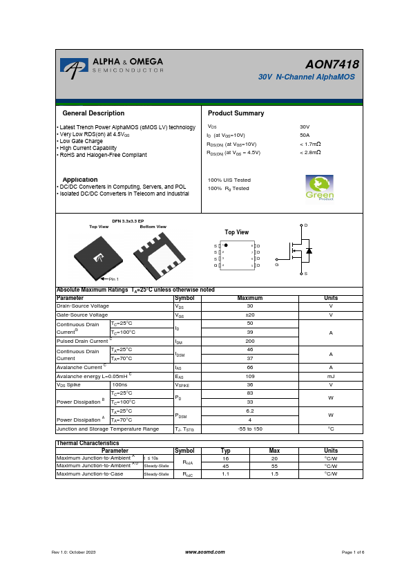
• Latest Trench Power AlphaMOS (αMOS LV) technology • Very Low RDS(on) at 4.5VGS • Low Gate Charge • High Current Capability • RoHS and Halogen-Free Compliant Product Summary VDS ID (at VGS=10V) RDS(ON) (at VGS=10V) RDS(ON) (at VGS = 4.5V) Application • DC/DC Converters in Computing, Servers, and POL • Isolated DC/DC Converters in Telecom and Industrial 100% UIS Tested 100% Rg Tested 30V 50A < 1.7mW < 2.8mW DFN 3.3x3.3 EP Top View Bottom View Top View S1 S2 S3 G4 8D 7D 6D 5D G Pin 1 Absolute Maximum Ratings TA=25°C unless otherwise noted Parameter Symbol Drain-Source Voltage VDS Gate-Source Voltage VGS Continuous Drain CurrentG TC=25°C TC=100°C ID Pulsed Drain Current C IDM Continuous Drain Current TA=25°C TA=70°C IDSM Avalanche Current C IAS Avalanche energy L=0.05mH C EAS VDS Spike 100ns VSPIKE TC=25°C Power Dissipation B TC=100°C PD TA=25°C Power Dissipation A TA=70°C PDSM Junction and Storage Temperature Range TJ, TSTG Maximum 30 ±20 50 39 200 46 37 66 109 36 83 33 6.2 4 -55 to 150 Thermal Characteristics Parameter Symbol Typ Maximum Junction-to-Ambient A t ≤ 10s Maximum Junction-to-Ambient A D Steady-State RqJA 16 45 Maximum Junction-to-Case Steady-State RqJC 1.1 Max 20 55 1.5 D S Units V V A A A mJ V W W °C Units °C/W °C/W °C/W Rev 1.0: October 2023 www.aosmd.com Page 1 of 6 AON7418 Electrical Characteristics (TJ=25°C unless otherwise noted) Symbol Parameter Conditions Min Typ Max Units STATIC PARAMETERS BVDSS Drain-Source Breakdown Voltage ID=250mA, VGS=0V 30 V IDSS Zero Gate Voltage Drain Current VDS=30V, VGS=0V TJ=55°C 1 5 mA IGSS Gate-Body leakage current VDS=0V, VGS= ±20V 100 nA VGS(th) Gate Threshold Voltage VDS=VGS,ID=250mA 1.2 1.8 2.2 V RDS(ON) Static Drain-Source On-Resistance VGS=10V, ID=20A TJ=125°C 1.4 1.7 2.1 2.6 mW VGS=4.5V, ID=20A 2.2 2.8 mW gFS Forward Transconductance VDS=5V, ID=20A 153 S VSD
AON7418 30V N-Channel AlphaMOS General.
| Part Number | Description |
|---|---|
| AON7410 | 30V N-Channel MOSFET |
| AON7412 | 30V N-Channel MOSFET |
| AON7414 | 30V N-Channel MOSFET |
| AON7416 | 30V N-Channel MOSFET |
| AON7400 | Field Effect Transistor |
| AON7400A | 30V N-Channel MOSFET |
| AON7401 | 30V P-Channel MOSFET |
| AON7402 | 30V N-Channel MOSFET |
| AON7403 | 30V P-Channel MOSFET |
| AON7404 | 20V N-Channel MOSFET |