Datasheet Details
| Part number | AOP605L |
|---|---|
| Manufacturer | Alpha & Omega Semiconductors |
| File Size | 575.25 KB |
| Description | MOSFET |
| Datasheet |
 AOP605L Datasheet AOP605L Datasheet
|
|
|
Download the AOP605L datasheet PDF. This datasheet also covers the AOP605 variant, as both devices belong to the same mosfet family and are provided as variant models within a single manufacturer datasheet.
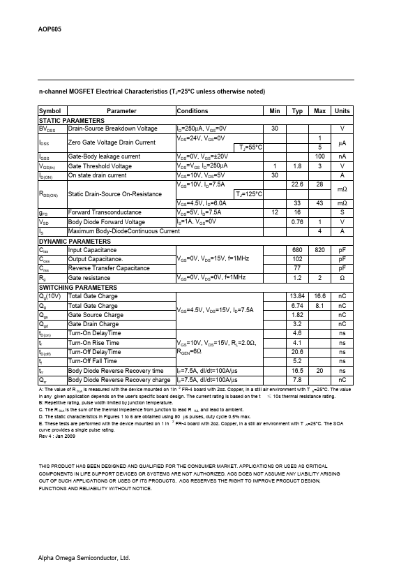
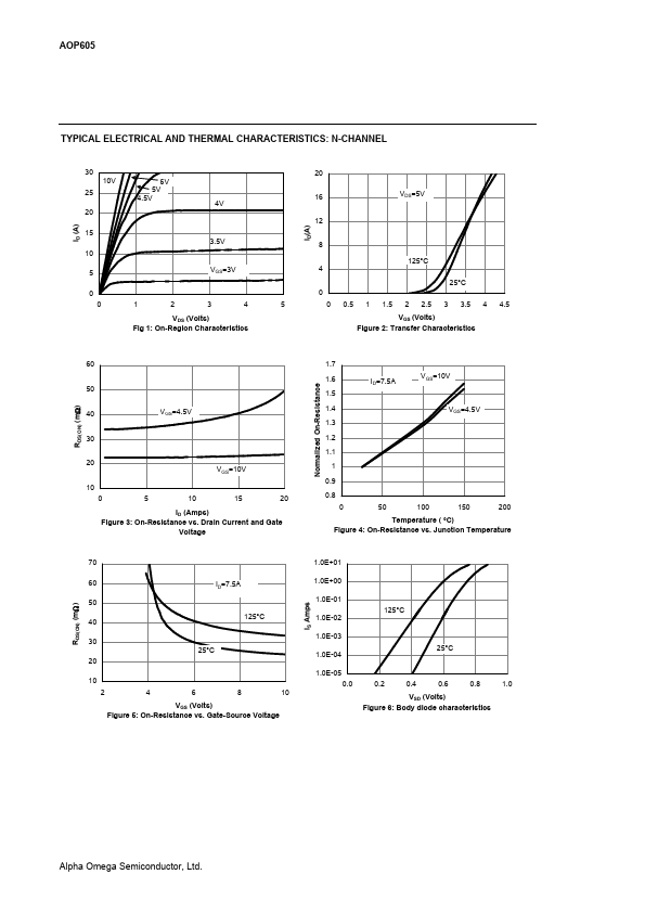
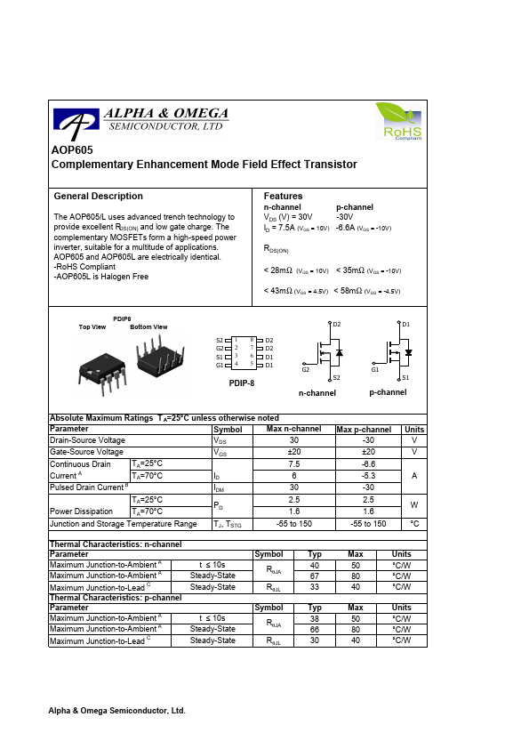
The AOP605/L uses advanced trench technology to provide excellent RDS(ON) and low gate charge.
The complementary MOSFETs form a high-speed power inverter, suitable for a multitude of applications.
AOP605 and AOP605L are electrically identical.
| Part number | AOP605L |
|---|---|
| Manufacturer | Alpha & Omega Semiconductors |
| File Size | 575.25 KB |
| Description | MOSFET |
| Datasheet |
AOP605L Datasheet
|
|
|
|
| Part Number | Description | Manufacturer |
|---|---|---|
| AOP604 | MOSFET | ETC |
| AOP1203-1001 | Mini LED Modules | Amperor |
| AOP1203-1002 | Mini LED Modules | Amperor |
| AOP1203-2001 | Mini LED Modules | Amperor |
| Part Number | Description |
|---|---|
| AOP605 | MOSFET |
| AOP600 | MOSFET |
| AOP601 | MOSFET |
| AOP606 | MOSFET |
| AOP607 | MOSFET |
The following content is an automatically extracted verbatim text from the original manufacturer datasheet and is provided for reference purposes only.