Datasheet Details
| Part number | AOTF20N40L |
|---|---|
| Manufacturer | Alpha & Omega Semiconductors |
| File Size | 419.77 KB |
| Description | 20A N-Channel MOSFET |
| Datasheet | AOTF20N40L AOTF20N40 Datasheet (PDF) |
|
|
Overview: AOTF20N40/AOTF20N40L 400V,20A N-Channel MOSFET General.
This datasheet includes multiple variants, all published together in a single manufacturer document.
| Part number | AOTF20N40L |
|---|---|
| Manufacturer | Alpha & Omega Semiconductors |
| File Size | 419.77 KB |
| Description | 20A N-Channel MOSFET |
| Datasheet | AOTF20N40L AOTF20N40 Datasheet (PDF) |
|
|
|
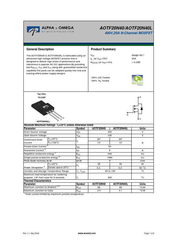
Product Summary The AOTF20N40 & AOTF20N40L is fabricated using an advanced high voltage MOSFET process that is designed to deliver high levels of performance and robustness in popular AC-DC applications.By providing low RDS(on), Ciss and Crss along with guaranteed avalanche capability this parts can be adopted quickly into new and existing offline power supply designs.
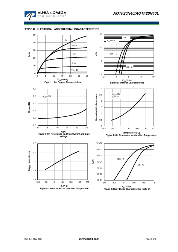
VDS ID (at VGS=10V) RDS(ON) (at VGS=10V) 100% UIS Tested 100% Rg Tested Top View TO-220F 500@150℃ 20A < 0.25W D G AOTF20N40(L) S GD Absolute Maximum Ratings TA=25°C unless otherwise noted Parameter Symbol AOTF20N40 AOTF20N40L Drain-Source Voltage VDS 400 Gate-Source Voltage VGS ±30 Continuous Drain Current TC=25°C TC=100°C ID 20* 20* 13* 13* Pulsed Drain Current C Avalanche Current C Repetitive avalanche energy C Single pulsed avalanche energy G Peak diode recovery dv/dt IDM IAR EAR EAS dv/dt 54 6 540 1080 5 TC=25°C Power Dissipation B Derate above 25oC PD 50 0.4 40 0.3 Junction and Storage Temperature Range TJ, TSTG -55 to 150 Maximum lead temperature for soldering purpose, 1/8" from case for 5 seconds TL 300 Thermal Characteristics Parameter Symbol Maximum Junction-to-Ambient A,D RqJA Maximum Junction-to-Case RqJC * Drain current limited by maximum junction temperature.
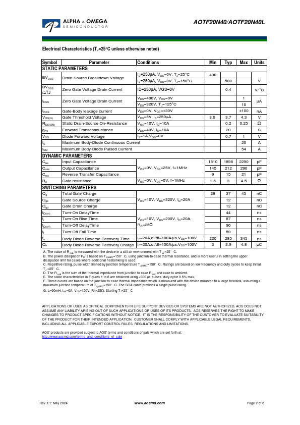
AOTF20N40 65 2.5 AOTF20N40L 65 3.1 S Units V V A A mJ mJ V/ns W W/ oC °C °C Units °C/W °C/W Rev 1.1: May 2024 www.aosmd.com Page 1 of 6 AOTF20N40/AOTF20N40L Electrical Characteristics (TJ=25°C unless otherwise noted) Symbol Parameter Conditions Min Typ Max Units STATIC PARAMETERS BVDSS Drain-Source Breakdown Voltage ID=250μA, VGS=0V, TJ=25°C ID=250μA, VGS=0V, TJ=150°C BVDSS /∆TJ Zero Gate Voltage Drain Current ID=250μA, VGS=0V IDSS Zero Gate Voltage Drain Current VDS=400V, VGS=0V VDS=320V, TJ=125°C IGSS Gate-Body leakage current VDS=0V, VGS=±30V VGS(th) Gate Threshold Voltage VDS=5V, ID=250mA
| Brand Logo | Part Number | Description | Manufacturer |
|---|---|---|---|
| AOTF20N40 | N-Channel MOSFET | INCHANGE |
| Part Number | Description |
|---|---|
| AOTF20N40 | 20A N-Channel MOSFET |
| AOTF20N60 | 20A N-Channel MOSFET |
| AOTF20C60 | N-Channel MOSFET |
| AOTF20S60 | Power Transistor |
| AOTF20S60L | Power Transistor |
| AOTF2142L | N-Channel MOSFET |
| AOTF2144L | 40V N-Channel MOSFET |
| AOTF2146L | 40V N-Channel MOSFET |
| AOTF2210L | N-Channel MOSFET |
| AOTF22N50 | 22A N-Channel MOSFET |