Datasheet Details
| Part number | AOD419 |
|---|---|
| Manufacturer | Alpha & Omega |
| File Size | 145.40 KB |
| Description | P-Channel MOSFET |
| Datasheet |
 AOD419 Datasheet AOD419 Datasheet
|
|
|
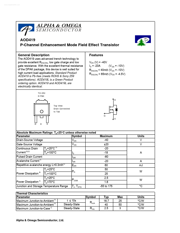
The AOD419 uses advanced trench technology to provide excellent RDS(ON), low gate charge and low gate resistance.
With the excellent thermal resistance of the DPAK package, this device is well suited for high current load applications.
| Part number | AOD419 |
|---|---|
| Manufacturer | Alpha & Omega |
| File Size | 145.40 KB |
| Description | P-Channel MOSFET |
| Datasheet |
AOD419 Datasheet
|
|
|
|