Datasheet Details
| Part number | AOD4191L |
|---|---|
| Manufacturer | Alpha & Omega Semiconductors |
| File Size | 546.54 KB |
| Description | P-Channel MOSFET |
| Download | AOD4191L Download (PDF) |
|
|
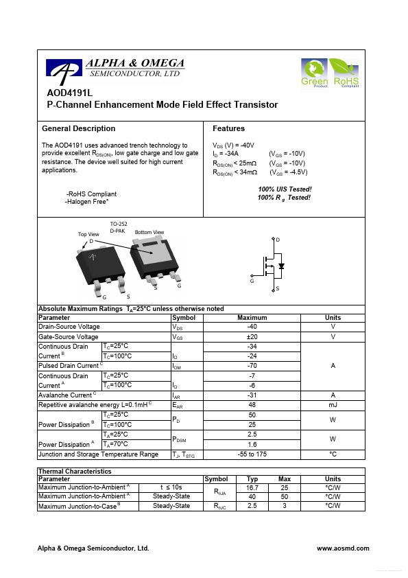
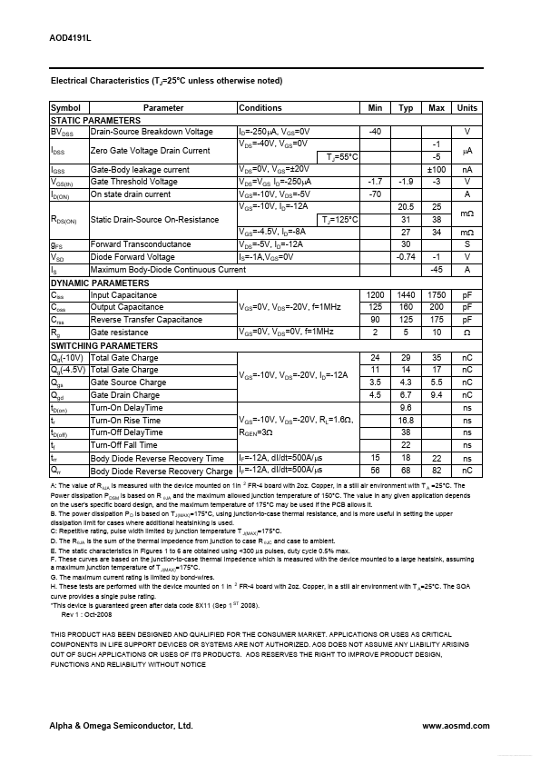
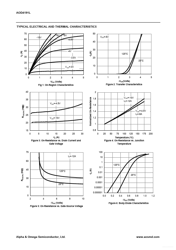
Overview: AOD4191L P-Channel Enhancement Mode Field Effect Transistor General.
| Part number | AOD4191L |
|---|---|
| Manufacturer | Alpha & Omega Semiconductors |
| File Size | 546.54 KB |
| Description | P-Channel MOSFET |
| Download | AOD4191L Download (PDF) |
|
|
|
The AOD4191 uses advanced trench technology to provide excellent RDS(ON), low gate charge and low gate resistance.
The device well suited for high current applications.
| Part Number | Description |
|---|---|
| AOD410 | N-Channel MOSFET |
| AOD4100 | N-Channel MOSFET |
| AOD4102 | 30V N-Channel MOSFET |
| AOD4104 | N-Channel MOSFET |
| AOD4106 | N-Channel MOSFET |
| AOD410L | N-Channel MOSFET |
| AOD4110 | N-Channel MOSFET |
| AOD4112 | N-Channel MOSFET |
| AOD412 | N-Channel MOSFET |
| AOD4120 | N-Channel MOSFET |