ADCMP600
ADCMP600 is Single-Supply TTL/CMOS Comparator manufactured by Analog Devices.
..
Preliminary Technical Data
Features
Rail-to-Rail, Very Fast, 2.5 V to 5.5 V, Single-Supply TTL/CMOS parators ADCMP600/ADCMP601/ADCMP602
FUNCTIONAL BLOCK DIAGRAM
NONINVERTING INPUT
10 m V sensitivity rail to rail at VCC = 2.5 V Input mon-mode voltage from
- 0.2 V to VCC + 0.2 V Low glitch CMOS-/TTL-patible output stage 3 ns propagation delay 15 m W at 3.3 V Shutdown pin Single-pin control for programmable hysteresis and latch Power supply rejection > 60 d B Improved replacement for MAX999
- 40°C to +125°C operation
INVERTING INPUT
ADCMP600/ ADCMP601/ ADCMP602
Q OUTPUT
LE/HYS (Except ADCMP600)
SDN (ADCMP602 Only)
Figure 1.
APPLICATIONS
High speed instrumentation Clock and data signal restoration Logic level shifting or translation Pulse spectroscopy High speed line receivers Threshold detection Peak and zero-crossing detectors High speed trigger circuitry Pulse-width modulators Current-/voltage-controlled oscillators Automatic test equipment (ATE)
GENERAL DESCRIPTION
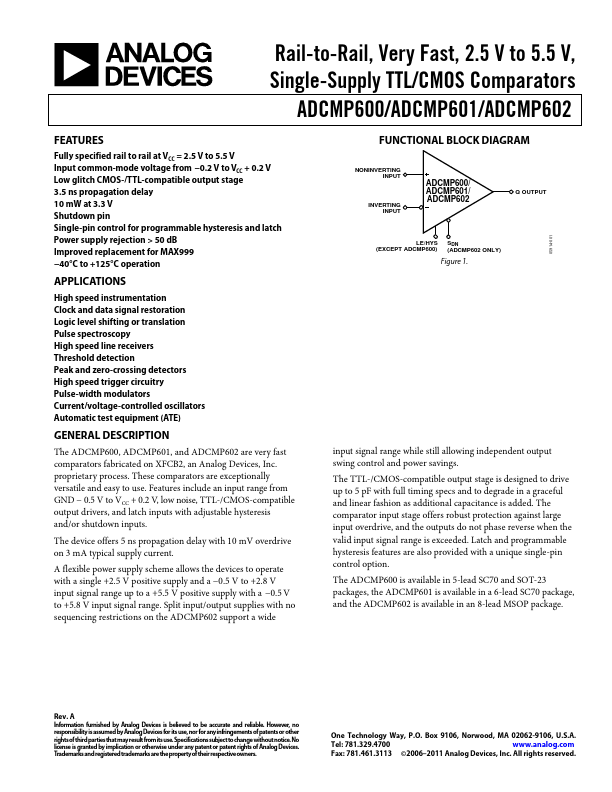
The ADCMP600, ADCMP601, and ADCMP602 are very fast parators fabricated on Analog Devices’ proprietary XFCB2 process. These parators are exceptionally versatile and easy to use. Features include an input range from VEE
- 0.5 V to VCC + 0.5 V, low noise TTL-/CMOS-patible output drivers, and latch inputs with adjustable hysteresis and/or shutdown inputs. The devices offer 3 ns propagation delay with 5 m V overdrive on 4 m A typical supply current. A flexible power supply scheme allows the devices to operate with a single +2.5 V positive supply and a
- 0.5 V to +3.0 V input signal range up to a +5.5 V positive supply with a
- 0.5 V to +6 V input signal range. Split input/output supplies with no sequencing restrictions on the ADCMP602 support a wide input signal range while still allowing independent output swing control and power savings. The TTL-/CMOS-patible output stage is designed to drive up to 5 p F with full timing specs and to degrade in a graceful and...