ADCMP609
FEATURES
10 m V sensitivity rail to rail at VCC = 2.5 V Input mon-mode voltage from
- 0.2 V to VCC + 0.2 V Low glitch CMOS-/TTL-patible output stage 30 ns propagation delay 1 m W at 2.5 V Shutdown pin Single-pin control for programmable hysteresis and latch Power supply rejection >60 d B
- 40C° to +125C° operation
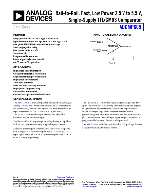
FUNCTIONAL BLOCK DIAGRAMS
NONINVERTING INPUT +
ADCMP608
INVERTING INPUT
- Q OUTPUT
APPLICATIONS
High speed instrumentation Clock and data signal restoration Logic level shifting or translation High speed line receivers Threshold detection Peak and zero-crossing detectors High speed trigger circuitry Pulse-width modulators Current-/voltage-controlled oscillators
NONINVERTING INPUT
+
Q OUTPUT Q OUTPUT
INVERTING INPUT
- LE/HYS
Figure 1.
GENERAL DESCRIPTION
The ADCMP608 and ADCMP609 are fast parators fabricated on Analog Devices’ proprietary XFCB2 process. These parators are exceptionally versatile and easy to use. Features include an input range from...