ADN2860
ADN2860 is 3-Channel Digital Potentiometer with Nonvolatile Memory manufactured by Analog Devices.
FEATURES
3 Channels:
3-Channel Digital Potentiometer with Nonvolatile Memory
Preliminary Technical Data
Dual 512-Position Single 128-Position 25KΩ or 150KΩ Full-Scale Resistance Low Temperature Coefficient: 35ppm/°C Nonvolatile Memory Retains Wiper Settings Permanent Memory Write-Protection Linear Increment/Decrement Log taper Increment/Decrement I2C patible Serial Interface 3V to 5V Single Supply Operation ±2.5V Dual Supply Operation 256 Bytes General Purpose User EEPROM 11 Bytes RDAC user EEPROM GBIC and SFP pliant EEPROM 100-year Typical Data Retention at TA=55°C APPLICATIONS Laser Diode Drivers Optical Amplifiers TIA Gain Setting TEC Controller Temperature Set Points
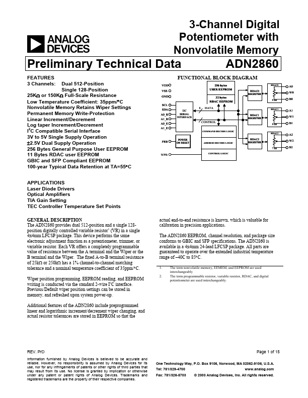
GENERAL DESCRIPTION
The ADN2860 provides dual 512-position and a single 128position digitally controlled variable resistor1 (VR) in a single 4x4mm LFCSP package. This device performs the same electronic adjustment function as a potentiometer, trimmer, or variable resistor. Each VR offers a pletely programmable value of resistance between the A terminal and the Wiper or the B terminal and the Wiper. The fixed A-to-B terminal resistance of 25kΩ or 250kΩ has a 1% channel-to-channel matching tolerance and a nominal temperature coefficient of 35ppm/°C. Wiper position programming, EEPROM reading, and EEPROM writing is conducted via the standard 2-wire I2C interface. Previous/Default wiper position settings can be stored in memory, and refreshed upon system power-up. Additional features of the ADN2860 include preprogrammed linear and logarithmic increment/decrement wiper changing, and actual resistor tolerances are stored in EEPROM so that the
VDD VSS GND SCL SDA A0_R A1_R A0_E A1_E
256 bytes USER EEPROM 32 bytes RDAC EEPROM
RDAC0
FUNCTIONAL BLOCK DIAGRAM
A0 W0
9 bit
RDAC1
RDAC0 REGISTER
B0
I2C SERIAL INTERFACE
DATA
RDAC1 REGISTER
A1 W1
CONTROL
MAND DECODE LOGIC
9 bit
RDAC2
B1
A2 W2
POWER ON RESET
ADDRESS DECODE LOGIC
RDAC2 REGISTER 7 bit
B2
CONTROL LOGIC actual...