ADN2865
ADN2865 is Clock and Data Recovery manufactured by Analog Devices.
FEATURES
Serial data input: 12.3 Mb/s to 2.7 Gb/s Exceeds ITU-T Jitter Specifications Integrated Limiting Amp: 6m V sensitivity Adjustable slice level: ±100 m V Patented dual-loop clock recovery architecture Programmable LOS detect and Slice Level Integrated PRBS Generator and Detector No reference clock required Loss of lock indicator Rate Selectivity without the use of a reference clock I2C™ interface to access optional features
Single-supply operation: 3.3 V Low power: 1.0W 8 mm × 8 mm 56-lead LFCSP
PRODUCT DESCRIPTION
The ADN2865 provides the receiver functions of quantization, signal level detect, and clock and data recovery for continuous data rates from 12.3 Mb/s to 2.7 Gb/s. An integrated deserialiser supports 8 bit parallel transfer to an FPGA or digital ASIC. The recovered clock can simultaneously serialize data supplied in an 8 bit parallel format. The ADN2865 automatically locks to all data rates without the need for an external reference clock or programming. All SONET jitter requirements are exceeded, including jitter transfer, jitter generation, and jitter tolerance. All specifications are quoted for
- 40°C to +85°C ambient temperature, unless otherwise noted. This device, together with a PIN diode and a TIA preamplifier, can implement a highly integrated, low cost, low power fiber optic receiver. The ADN2865 have many optional features available via an I2C interface, e.g. the user can read back the data rate that the ADN2865 is locked on to, or the user can set the device to only lock to one particular data rate if provisioning of data rates is required.
APPLICATIONS
Passive Optical Network s SONET OC-1/3/12/48 and all associated FEC rates Fibre Channel, 2× Fibre Channel , Gb E, HDTV, etc. WDM transponders Test equipment
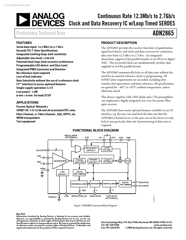
FUNCTIONAL BLOCK DIAGRAM
Figure 1 ADN2865 Functional Block Diagram
Rev.Pr A
Information furnished by Analog Devices is believed to be accurate and reliable. However, no responsibility is assumed by Analog Devices for its...