AD9520-0 Description
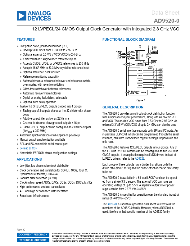
The AD9520-0 provides a multi-output clock distribution function with subpicosecond jitter performance, along with an on-chip PLL and VCO. The on-chip VCO tunes from 2.53 GHz to 2.95 GHz. An external 3.3 V/5 V VCO/VCXO of up to 2.4 GHz can also be used.
AD9520-0 Key Features
- Low phase noise, phase-locked loop (PLL)
- On-chip VCO tunes from 2.53 GHz to 2.95 GHz
- Optional external 3.3 V/5 V VCO/VCXO to 2.4 GHz
- 1 differential or 2 single-ended reference inputs
- Accepts CMOS, LVDS, or LVPECL references to 250 MHz
- Accepts 16.62 MHz to 33.3 MHz crystal for reference input
- Optional reference clock doubler
- Reference monitoring capability
- Automatic/manual reference holdover and reference switchover modes, with revertive switching
- Glitch-free switchover between references