BCW66F
Overview
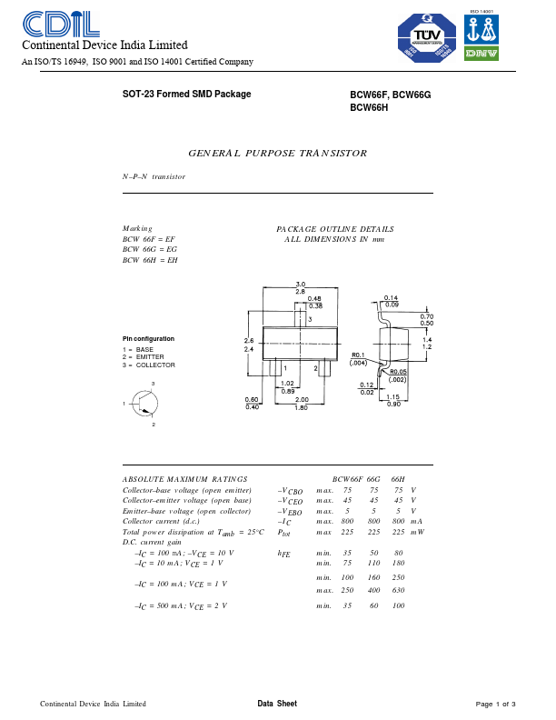
Continental Device India Limited An ISO/TS 16949, ISO 9001 and ISO 14001 Certified Company SOT-23 Formed SMD Package BCW66F, BCW66G BCW66H GENERAL PURPOSE TRANSISTOR N–P–N transistor Marking BCW 66...
| Part | BCW66F |
|---|---|
| Description | Transistor |
| Category | Transistor |
| Manufacturer | Continental Device India |
| Size | 77.38 KB |
Continental Device India Limited An ISO/TS 16949, ISO 9001 and ISO 14001 Certified Company SOT-23 Formed SMD Package BCW66F, BCW66G BCW66H GENERAL PURPOSE TRANSISTOR N–P–N transistor Marking BCW 66...
| Part Number | Manufacturer | Description |
|---|---|---|
| BCW66F | Infineon | NPN Silicon AF Transistor |
| BCW66F | Diotec Semiconductor | SMD General Purpose NPN Transistors |
| BCW66F | Motorola Semiconductor | GENERAL PURPOSE TRANSISTOR |
| BCW66F | NXP Semiconductors | NPN general-purpose transistor |
| BCW66F | Rectron | NPN Transistor |