BCW68
Key Features
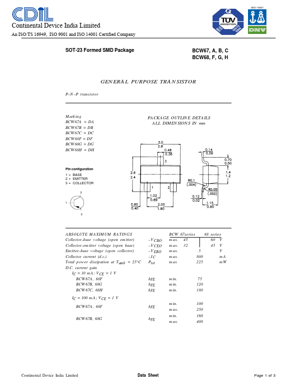
- P transistor
- base voltage (open emitter) Collector
| Part Number | Manufacturer | Description |
|---|---|---|
| BCW68G | Infineon | PNP Transistor |
| BCW68F | Infineon | PNP Transistor |
| BCW68G | Micro Commercial Components | PNP Transistor |
| BCW68F | Multicomp | PNP Transistor |
| BCW68 | Multicomp | PNP Transistor |
| BCW68 | SeCoS Halbleitertechnologie GmbH | PNP Transistor |
| BCW68F | SeCoS Halbleitertechnologie GmbH | PNP Transistor |
| BCW68 | SEMTECH | PNP Transistor |
| BCW68F | SEMTECH | PNP Transistor |
| BCW68H | SEMTECH | PNP Transistor |