APPLICATIONS
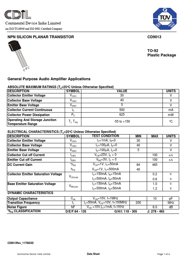
ABSOLUTE MAXIMUM RATINGS
(Ta=25ºC Unless Otherwise Specified) VALUE DESCRIPTION
SYMBOL V 30 Collector Emitter Voltage CEO V 40 Collector Base Voltage CBO VEBO 5 Emitter Base Voltage Collector Current Continuous Collector Power Dissipation Operating And Storage Junction Temperature Range IC PC Tj, Tstg 500 625 -55 to +150 UNITS V V V mA mW ºC ELECTRICAL CHARACTERISTICS
(Ta=25ºC Unless Otherwise Specified) TEST CONDITION DESCRIPTION
SYMBOL IC=1mA, IB=0 V Collector Emitter Voltage CEO VCBO IC=100µA, IE=0 Collector Base Voltage Emitter Base Voltage Collector Cut off Current Emitter Cut off Current DC Current Gain Collector Emitter Saturation Voltage Base Emitter Saturation Voltage DYNAMIC CHARACTERISTICS Output Capacitance Transition Frequency Noise Figure *hFE CLASSIFICATION VEBO ICBO IEBO *hFE hFE VCE(sat) VBE(sat) IE=100µA, IC=0 VCB=25V, IE = 0 VBE=3V, IC = 0 VCE=1V, IC=50mA VCE=1V, IC=500mA IC=150mA, IB=15mA IC=500mA, IB=50mA IC=150mA, IB=15mA IC=500mA, IB=50mA MIN 30 40 5... Continental Device India