CEK01N7 Overview
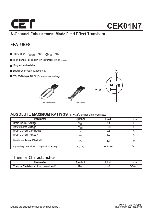
CEK01N7 N-Channel Enhancement Mode Field Effect Transistor.
| Part number | CEK01N7 |
|---|---|
| Datasheet | CEK01N7-CET.pdf |
| File Size | 345.51 KB |
| Manufacturer | CET |
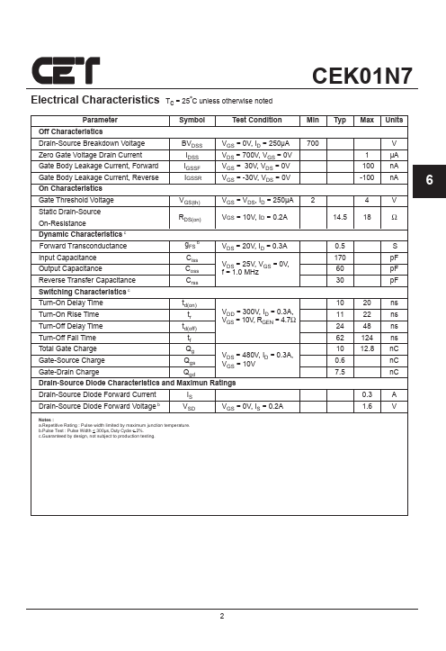
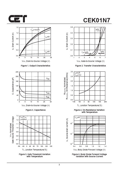
| Description | N-Channel MOSFET |
|
|
CEK01N7 N-Channel Enhancement Mode Field Effect Transistor.