Click to expand full text
www.DataSheet.co.kr
N-Channel Enhancement Mode Field Effect Transistor FEATURES
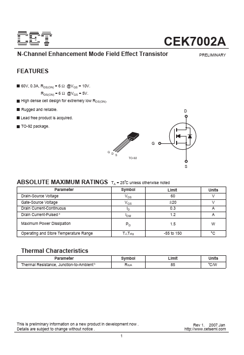
60V, 0.3A, RDS(ON) = 6 Ω @VGS = 10V. RDS(ON) = 6 Ω @VGS = 5V. High dense cell design for extremely low RDS(ON). Rugged and reliable. Lead free product is acquired. TO-92 package.
CEK7002A
PRELIMINARY
D
G
G D S
TO-92
S
ABSOLUTE MAXIMUM RATINGS
Parameter Drain-Source Voltage Gate-Source Voltage Drain Current-Continuous Drain Current-Pulsed
a
TA = 25 C unless otherwise noted Symbol VDS VGS ID IDM PD TJ,Tstg Limit 60 Units V V A A W C
±20
0.3 1.2 1.5 -55 to 150
Maximum Power Dissipation Operating and Store Temperature Range
Thermal Characteristics
Parameter Thermal Resistance, Junction-to-Ambient b Symbol RθJA Limit 85 Units C/W
This is preliminary information on a new product in development now .