CEP20P10 Overview
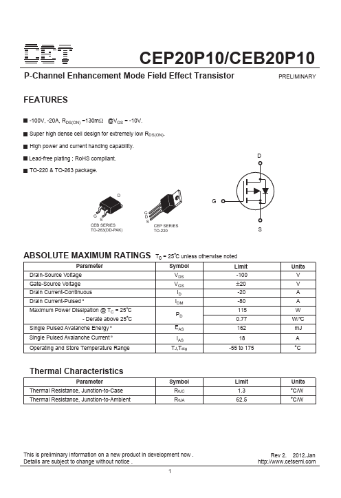
CEP20P10/CEB20P10 P-Channel Enhancement Mode Field Effect Transistor PRELIMINARY.
CEP20P10 Key Features
- 100V, -20A, RDS(ON) =130mΩ @VGS = -10V. Super high dense cell design for extremely low RDS(ON). High power and current h
CEP20P10 datasheet by CET.
| Part number | CEP20P10 |
|---|---|
| Datasheet | CEP20P10-CET.pdf |
| File Size | 372.75 KB |
| Manufacturer | CET |
| Description | P-Channel Enhancement Mode Field Effect Transistor |
|
|
CEP20P10/CEB20P10 P-Channel Enhancement Mode Field Effect Transistor PRELIMINARY.
| Part Number | Description |
|---|---|
| CEP20P06 | P-Channel MOSFET |
| CEP20A03 | N-Channel Enhancement Mode Field Effect Transistor |
| CEP20N06 | N-Channel MOSFET |
| CEP21A2 | N-Channel MOSFET |
| CEP21A3 | N-Channel MOSFET |
| CEP01N6 | N-Channel MOSFET |
| CEP01N65 | N-Channel MOSFET |
| CEP01N6G | N-Channel MOSFET |
| CEP02N65A | N-Channel Enhancement Mode Field Effect Transistor |
| CEP02N65D | N-Channel MOSFET |