Datasheet4U Logo Datasheet4U.com

CEP20A03 - N-Channel Enhancement Mode Field Effect Transistor

Key Features

  • 30V, 197A, RDS(ON) = 2 mΩ @VGS = 10V. RDS(ON) = 3 mΩ @VGS = 4.5V. Super high dense cell design for extremely low RDS(ON). High power and current handing capability. Lead-free plating ; RoHS compliant. TO-220 & TO-263 package. D D G S CEB SERIES TO-263(DD-PAK) G D S CEP SERIES TO-220 G S.

📥 Download Datasheet

Datasheet Details

Part number CEP20A03
Manufacturer CET
File Size 396.44 KB
Description N-Channel Enhancement Mode Field Effect Transistor
Datasheet download datasheet CEP20A03 Datasheet

Full PDF Text Transcription (Reference)

The following content is an automatically extracted verbatim text from the original manufacturer datasheet and is provided for reference purposes only.

View original datasheet text
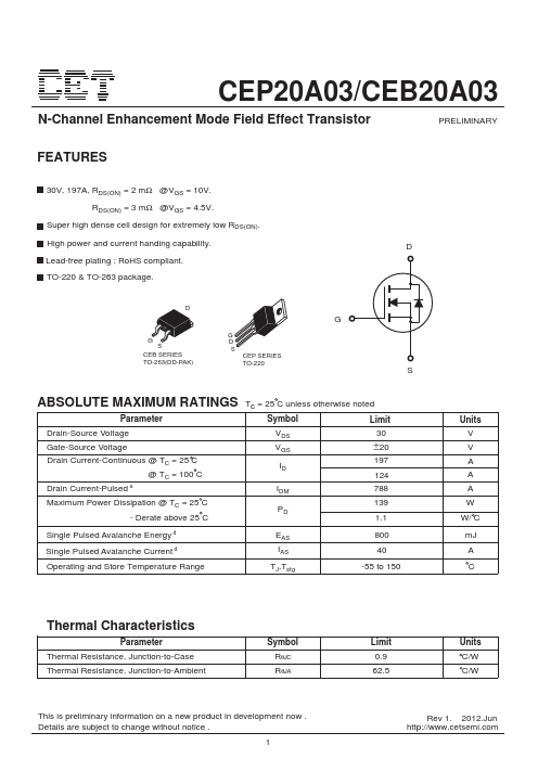
CEP20A03/CEB20A03 N-Channel Enhancement Mode Field Effect Transistor PRELIMINARY FEATURES 30V, 197A, RDS(ON) = 2 mΩ @VGS = 10V. RDS(ON) = 3 mΩ @VGS = 4.5V. Super high dense cell design for extremely low RDS(ON). High power and current handing capability. Lead-free plating ; RoHS compliant. TO-220 & TO-263 package. D D G S CEB SERIES TO-263(DD-PAK) G D S CEP SERIES TO-220 G S ABSOLUTE MAXIMUM RATINGS Tc = 25 C unless otherwise noted Parameter Symbol Limit Drain-Source Voltage Gate-Source Voltage Drain Current-Continuous @ TC = 25 C @ TC = 100 C Drain Current-Pulsed a Maximum Power Dissipation @ TC = 25 C - Derate above 25 C VDS VGS ID IDM PD 30 ±20 197 124 788 139 1.