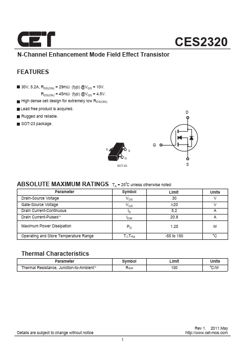
The following content is an automatically extracted verbatim text
from the original manufacturer datasheet and is provided for reference purposes only.
View original datasheet text
CES2320
N-Channel Enhancement Mode Field Effect Transistor
FEATURES
30V, 5.2A, RDS(ON) = 29mΩ (typ) @VGS = 10V. RDS(ON) = 45mΩ (typ) @VGS = 4.5V.
High dense cell design for extremely low RDS(ON). Lead free product is acquired. Rugged and reliable. SOT-23 package.
D
DS G
SOT-23
G
S
ABSOLUTE MAXIMUM RATINGS TA = 25 C unless otherwise noted
Parameter
Symbol
Limit
Drain-Source Voltage Gate-Source Voltage
VDS 30
VGS ±20
Drain Current-Continuous Drain Current-Pulsed a
ID 5.2 IDM 20.8
Maximum Power Dissipation
PD 1.25
Operating and Store Temperature Range
TJ,Tstg
-55 to 150
Thermal Characteristics
Parameter Thermal Resistance, Junction-to-Ambient b
Symbol RθJA
Limit 100
Units V V A A W C
Units C/W
Details are subject to change without notice
1
Rev 1. 2011.May http://www.