MTC3588BDFA6
MTC3588BDFA6 is P- & N-Channel Enhancement Mode Power MOSFET manufactured by CYStech Electronics.
CYStech Electronics Corp.
Spec. No. : C102DFA6 Issued Date : 2015.12.03 Revised Date : Page No. : 1/13
N- And P-Channel Enhancement Mode MOSFET
N-CH
BVDSS
14V
P-CH -14V
6A(VGS=4.5V)
-4A(VGS=-4.5 V)
16.6mΩ(VGS=4.5V) 43mΩ(VGS=-4.5V)
RDSON(TYP.)
23.7mΩ(VGS=2.5V) 38.5mΩ(VGS=1.8V)
63.6mΩ(VGS=-2.5V) 86.5mΩ(VGS=-1.8V)
66.3mΩ(VGS=1.5V) 153.3mΩ(VGS=-1.5V)
Description
The MTC3588BDFA6 consists of a N-channel and a P-channel enhancement-mode MOSFET in a single
DFN2- 2-6L package, providing the designer with the best bination of fast switching, ruggedized device design, low on-resistance and cost-effectiveness.
The DFN2- 2-6L package is universally preferred for all mercial-industrial surface mount applications.
Features
- Simple drive requirement
- Pb-free lead plating and halogen-free package
- Low on-resistance
- Fast switching speed
- Low gate charge
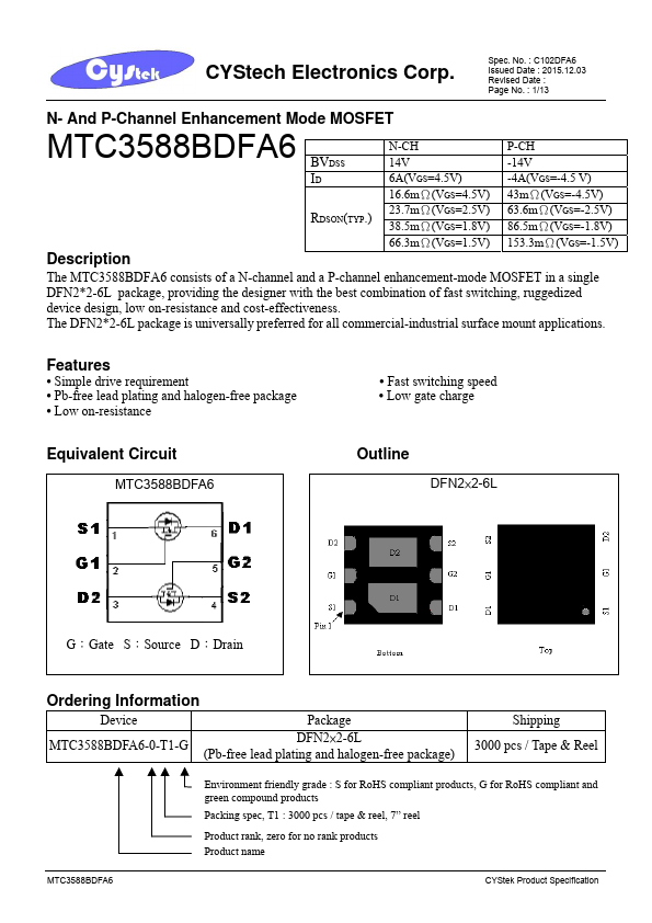
Equivalent Circuit
Outline
DFN2×2-6L
G:Gate S:Source...