Datasheet4U.com
🌙
MTN2306N3 Datasheet | CYStech
Part:
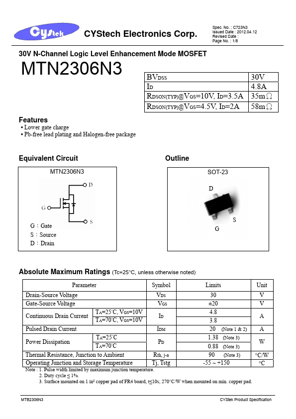
MTN2306N3
Description:
N-Channel Enhancement Mode MOSFET
Category:
MOSFET
Manufacturer:
CYStech
Size:
264.62 KB
MTN2306N3 Datasheet (PDF) Download
Related MTN2306N3 Datasheets
MTN2306ZN3 N-Channel Enhancement Mode MOSFET
MTN2306AM3 N-Channel MOSFET
MTN2306AN3 N-Channel Enhancement Mode MOSFET
CYStech
MTN2306N3
Key Features
Lower gate charge
Pb-free lead plating and Halogen-free package
×
Close