CAT28F512
CAT28F512 is 512K-Bit CMOS Flash Memory manufactured by Catalyst Semiconductor.
FEATURES s Fast Read Access Time: 90/120/150 ns s Low Power CMOS Dissipation:
Licensed Intel second source s mercial, Industrial and Automotive
Temperature Ranges s Stop Timer for Program/Erase s On-Chip Address and Data Latches s JEDEC Standard Pinouts:
- Active: 30 m A max (CMOS/TTL levels)
- Standby: 1 m A max (TTL levels)
- Standby: 100 µA max (CMOS levels) s High Speed Programming:
- 10 µs per byte
- 1 Sec Typ Chip Program s 12.0V
± 5% Programming and Erase Voltage
- 32-pin DIP
- 32-pin PLCC
- 32-pin TSOP ( 8 x 20) s 100,000 Program/Erase Cycles s 10 Year Data Retention s Electronic Signature
DESCRIPTION
The CAT28F512 is a high speed 64K x 8-bit electrically erasable and reprogrammable Flash memory ideally suited for applications requiring in-system or after-sale code updates. Electrical erasure of the full memory contents is achieved typically within 0.5 second. It is pin and Read timing patible with standard EPROM and E2PROM devices. Programming and Erase are performed through an operation and verify algorithm. The instructions are input via the I/O bus, using a two write cycle scheme. Address and Data are latched to free the I/O bus and address bus during the write operation. The CAT28F512 is manufactured using Catalyst’s advanced CMOS floating gate technology. It is designed to endure 100,000 program/erase cycles and has a data retention of 10 years. The device is available in JEDEC approved 32-pin plastic DIP, 32-pin PLCC or 32-pin TSOP packages.
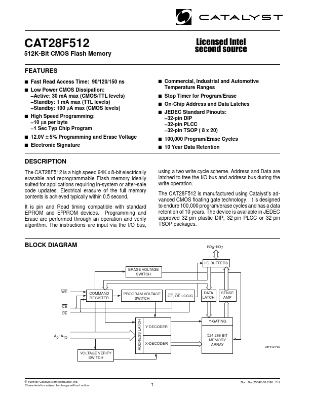
BLOCK DIAGRAM
I/O0- I/O7
I/O BUFFERS ERASE VOLTAGE SWITCH
MAND REGISTER
PROGRAM VOLTAGE SWITCH
CE, OE LOGIC
DATA LATCH
SENSE AMP
CE OE
ADDRESS LATCH
Y-GATING Y-DECODER 524,288 BIT MEMORY ARRAY
A0- A15
X-DECODER
28F512 F02
VOLTAGE VERIFY SWITCH
© 1998 by Catalyst Semiconductor, Inc. Characteristics subject to change without notice
Doc. No. 25042-00 2/98 F-1
Preliminary
PIN CONFIGURATION
PIN FUNCTIONS
Pin Name A0- A15 Type Input I/O Input Input Input Function Address Inputs for...