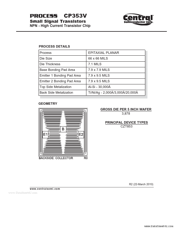
CP353V Description
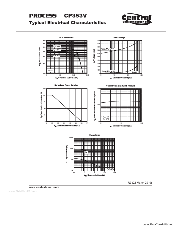
PROCESS CP353V Typical R2 (22-March 2010) w w.
CP353V Key Features
- s e m i . c o m .. PROCESS CP353V Typical
CP353V is Small Signal Transistors NPN - High Current Transistor Chip manufactured by Central Semiconductor .
| Part Number | Description |
|---|---|
| CP357X | Small Signal MOSFET Transistor N-Channel Enhancement-Mode MOSFET Chip |
| CP359R | Small Signal MOSFET N-Channel Enhancement-Mode MOSFET Chip |
| CP302-MPSH10 | NPN - RF Transistor Die |
| CP305 | Small Signal Transistor NPN - High Current Transistor Chip |
| CP305V-BCW66H | NPN Transistor |
PROCESS CP353V Typical R2 (22-March 2010) w w.