CEP06N5
CEP06N5 is N-Channel Logic Level Enhancement Mode Field Effect Transistor manufactured by Chino-Excel Technology.
- Part of the CEP06N5_Chino comparator family.
- Part of the CEP06N5_Chino comparator family.
FEATURES
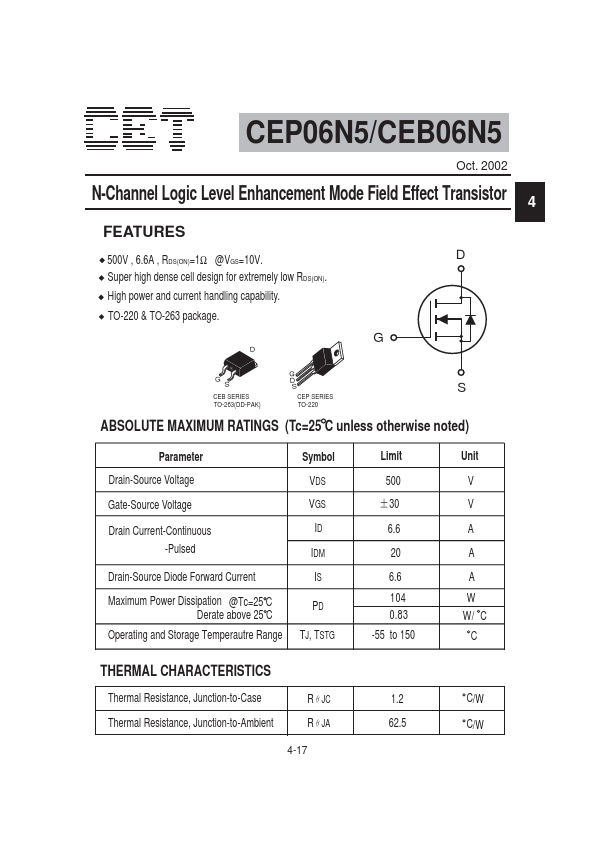
500V , 6.6A , RDS(ON)=1Ω @VGS=10V. Super high dense cell design for extremely low RDS(ON). High power and current handling capability. TO-220 & TO-263 package.
4 4
CEB SERIES TO-263(DD-PAK)
CEP SERIES TO-220
ABSOLUTE MAXIMUM RATINGS (Tc=25 C unless otherwise noted)
Parameter Drain-Source Voltage Gate-Source Voltage Drain Current-Continuous -Pulsed Drain-Source Diode Forward Current Maximum Power Dissipation @Tc=25 C Derate above 25 C Operating and Storage Temperautre Range Symbol VDS VGS ID IDM IS PD TJ, TSTG Limit 500 Unit V V A A A W W/ C C
Ć 30
6.6 20 6.6 104 0.83 -55 to 150
THERMAL CHARACTERISTICS
Thermal Resistance, Junction-to-Case Thermal Resistance, Junction-to-Ambient RįJC RįJA
4-17
1.2 62.5
C/W C/W
CEP06N5/CEB06N5
ELECTRICAL CHARACTERISTICS (TC=25 C unless otherwise noted)
4 4
Parameter
Single Pulse Drain-Source Avalanche Energy Maximum Drain-Source Avalanche Current
Symbol a
Condition
VDD =50V, L=24m H RG=25 Ω
Min Typ Max Unit
DRAIN-SOURCE AVALANCHE RATING
EAS IAS
500 6 m J A
OFF CHARACTERISTICS
Drain-Source Breakdown Voltage Zero Gate Voltage Drain Current Gate-Body Leakage BVDSS IDSS IGSS VGS(th) RDS(ON) ID(ON) g FS b
VGS = 0V,ID = 250µA VDS = 500V, VGS = 0V VGS = Ć30V, VDS = 0V VDS = VGS, ID = 250µA VGS =10V, ID = 4A VGS = 10V, VDS = 10V VDS = 50V, ID = 4A VDD =250V, ID = 6A, VGS = 10V RGEN=18Ω
500 25
V µA Ć100 n A
ON CHARACTERISTICS a
Gate Threshold Voltage Drain-Source On-State Resistance On-State Drain Current Forward Transconductance 2 4 0.85 1.0 6 4 23 35 44 54 VDS =400V, ID = 6A, VGS =10V
4-18
V Ω A S
SWITCHING CHARACTERISTICS
Turn-On Delay Time Rise Time Turn-Off Delay Time Fall Time Total Gate Charge Gate-Source Charge Gate-Drain Charge t D(ON) tr t D(OFF) tf Qg Qgs...