B9946
B9946 is 3.3V 160-MHz 1:10 Clock Distribution Buffer manufactured by Cypress.
Features
- -
- -
- -
- -
- 160-MHz Clock Support LVCMOS/LVTTL patible Inputs 10 Clock Outputs: Drive up to 20 Clock Lines 1X or 1/2X Configurable Outputs Output Three-state Control 250 ps Maximum Output-to-Output Skew Pin patible with MPC946 Industrial Temp. Range:
- 40°C to +85°C 32-Pin TQFP Package
Description
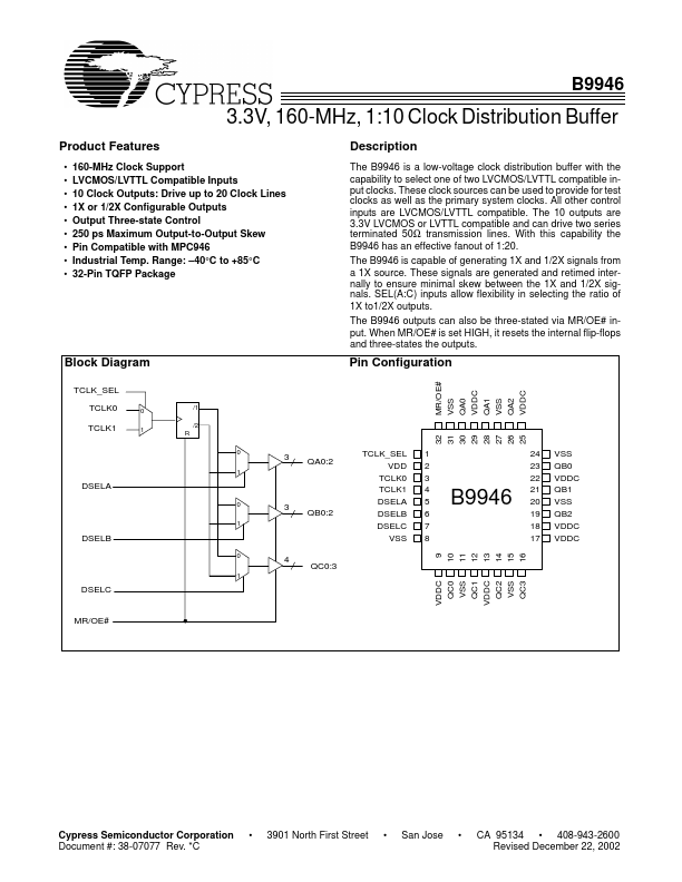
The B9946 is a low-voltage clock distribution buffer with the capability to select one of two LVCMOS/LVTTL patible input clocks. These clock sources can be used to provide for test clocks as well as the primary system clocks. All other control inputs are LVCMOS/LVTTL patible. The 10 outputs are 3.3V LVCMOS or LVTTL patible and can drive two series terminated 50Ω transmission lines. With this capability the B9946 has an effective fanout of 1:20. The B9946 is capable of generating 1X and 1/2X signals from a 1X source. These signals are generated and retimed internally to ensure minimal skew between the 1X and 1/2X signals. SEL(A:C) inputs allow flexibility in selecting the ratio of 1X to1/2X outputs. The B9946 outputs can also be three-stated via MR/OE# input. When MR/OE# is set HIGH, it resets the internal flip-flops and three-states the outputs.
Block Diagram
TCLK_SEL TCLK0 TCLK1
0 1 R 0 1 /1 /2
Pin Configuration
MR/OE# VSS QA0 VDDC QA1 VSS QA2 VDDC TCLK_SEL VDD TCLK0 TCLK1 DSELA DSELB DSELC VSS 1 2 3 4 5 6 7 8 32 31 30 29 28 27 26 25 24 23 22 21 20 19 18 17
QA0:2
DSELA
0 1
9 10 11 12 13 14 15 16
QB0:2
DSELB
0 1
VSS QB0 VDDC QB1 VSS QB2 VDDC VDDC
QC0:3
VDDC QC0 VSS QC1 VDDC QC2 VSS QC3
DSELC
MR/OE#
Cypress Semiconductor Corporation Document #: 38-07077 Rev.
- C
- 3901 North First Street
- San Jose
- CA 95134
- 408-943-2600 Revised December 22, 2002
Pin Description
[1]
Pin 3, 4 26, 28, 30 19, 21, 23 10, 12, 14, 16 5, 6, 7 1 32 Name TCLK(0,1) QA(2:0) QB(2:0) QC(0:3) DSEL(A:C) TCLK_SEL MR/OE# VDDC VDDC VDDC PWR I/O I, PU O O O I, PD I, PD I, PD Clock Outputs Clock Outputs Clock Outputs Divider Select Inputs. When HIGH,...