B9949
B9949 is 1:15 Clock Distribution Buffer manufactured by Cypress.
Features
- -
- -
- -
- -
- - 160MHz Clock Support LVPECL or LVCMOS/LVTTL Clock Input LVCMOS/LVTTL patible Inputs 15 Clock Outputs: Drive up to 30 Clock Lines 1X and 1/2X Configurable Outputs Output Three-state Control 350 ps Maximum Output-to-Output Skew Pin patible with MPC949 Industrial Temp. Range:
- 40°C to +85°C 52-Pin TQFP Package
Description
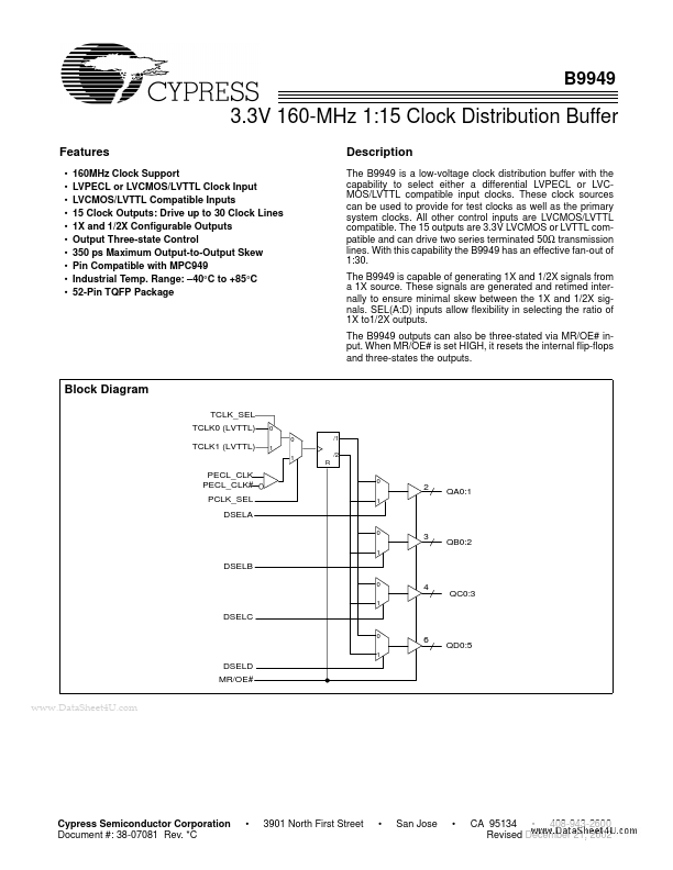
The B9949 is a low-voltage clock distribution buffer with the capability to select either a differential LVPECL or LVCMOS/LVTTL patible input clocks. These clock sources can be used to provide for test clocks as well as the primary system clocks. All other control inputs are LVCMOS/LVTTL patible. The 15 outputs are 3.3V LVCMOS or LVTTL patible and can drive two series terminated 50Ω transmission lines. With this capability the B9949 has an effective fan-out of 1:30. The B9949 is capable of generating 1X and 1/2X signals from a 1X source. These signals are generated and retimed internally to ensure minimal skew between the 1X and 1/2X signals. SEL(A:D) inputs allow flexibility in selecting the ratio of 1X to1/2X outputs. The B9949 outputs can also be three-stated via MR/OE# input. When MR/OE# is set HIGH, it resets the internal flip-flops and three-states the outputs.
Block Diagram
TCLK_SEL TCLK0 (LVTTL) TCLK1 (LVTTL) PECL_CLK PECL_CLK# PCLK_SEL DSELA
0 1
0 0 1 1 /2 R 0 1 /1
QA0:1
QB0:2
DSELB
0 1
QC0:3
DSELC
0 1
QD0:5
DSELD MR/OE#
..
Cypress Semiconductor Corporation Document #: 38-07081 Rev.
- C
- 3901 North First Street
- San Jose
- CA 95134
- 408-943-2600 Revised December 21, 2002
Pin Configuration
52 51 50 49 48 47 46 45 44 43 42 41 40 MR/OE# TCLK_SEL VDD TCLK0 TCLK1 PECL_CLK PECL_CLK# PCLK_SEL DSELA DSELB DSELC DSELD VSS 1 2 3 4 5 6 7 8 9 10 11 12 13 39 38 37 36 35 34 33 32 31 30 29 28 27 NC VSS QC0 VDDC QC1 VSS QC2 VDDC QC3 VSS VSS QD5 NC
14 15 16 17 18 19 20 21 22 23 24 25 26
NC VDDC QB2 VSS QB1 VDDC QB0 VSS VSS QA1 VDDC QA0 VSS
NC VDDC QD4 VSS QD3 VDDC QD2 VSS QD1 VDDC...