Datasheet Summary
Failsafe™ 2.5 V/3.3 V Zero Delay Buffer
Failsafe™ 2.5 V/3.3 V Zero Delay Buffer
Features
- Internal digital controlled crystal oscillator (DCXO) for continuous glitch-free operation
- Zero input-output propagation delay
- Low jitter (35 ps max RMS) outputs
- Low output-to-output skew (200 ps max)
- 4.17 MHz to 166.7 MHz reference input
- Supports industry standard input crystals
- 166.7 MHz outputs
- 5 V tolerant Inputs
- Phase-locked loop (PLL) bypass mode
- Dual reference inputs
- 16-Pin thin shrunk small outline package (TSSOP)
- 2.5 V or 3.3 V output power supplies
- 3.3 V core power supply
- Industrial temperature range
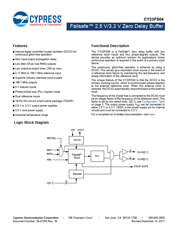
Logic Block Diagram
XIN XOUT
REFSEL
DCXO
Functional...