CY7C1049BV33
CY7C1049BV33 is 512K x 8 Static RAM manufactured by Cypress.
049BV33
512K x 8 Static RAM
Features
- High speed
- t AA = 15 ns
- Low active power
- 504 m W (max.)
- Low CMOS standby power (mercial L version)
- 1.8 m W (max.)
- 2.0V Data Retention (660 µW at 2.0V retention) ..
- Automatic power-down when deselected
- TTL-patible inputs and outputs
- Easy memory expansion with CE and OE Features expansion is provided by an active LOW Chip Enable (CE), an active LOW Output Enable (OE), and three-state drivers. Writing to the device is acplished by taking Chip Enable (CE) and Write Enable (WE) inputs LOW. Data on the eight I/O pins (I/O0 through I/O7) is then written into the location specified on the address pins (A0 through A18). Reading from the device is acplished by taking Chip Enable (CE) and Output Enable (OE) LOW while forcing Write Enable (WE) HIGH. Under these conditions, the contents of the memory location specified by the address pins will appear on the I/O pins. The eight input/output pins (I/O0 through I/O7) are placed in a high-impedance state when the device is deselected (CE HIGH), the outputs are disabled (OE HIGH), or during a write operation (CE LOW, and WE LOW). The CY7C1049BV33 is available in a standard 400-mil-wide 36-pin SOJ and 44-pin TSOPII packages with center power and ground (revolutionary) pinout.
Functional Description[1]
The CY7C1049BV33 is a high-performance CMOS Static RAM organized as 524,288 words by 8 bits. Easy memory
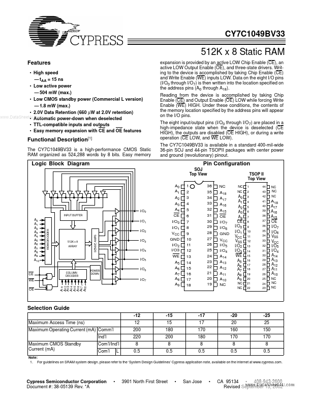
Logic Block Diagram
Pin Configuration
SOJ Top View
TSOP II Top View
NC A18 A17 A16 A15 OE I/O7 I/O6 GND VCC I/O5 I/O4 A14 A13 A12 A11 A10 NC
NC NC
1 2 3 4 5 6 7 8 9 10 11 12 13 14 15 16 17 18 19 20 21 22 44 43 42 41 40 39 38 37 36 35 34 33 32 31 30 29 28 27 26 25 24 23
I/O0
INPUT BUFFER
A0 A1 A2 A3 A4 A5 A6 A7 A8 A9 A10
I/O1
ROW DECODER
I/O2
SENSE AMPS
512K x 8...